IS45S16800E-7TLA1
| Part Description |
IC DRAM 128MBIT PAR 54TSOP II |
|---|---|
| Quantity | 721 Available (as of June 15, 2026) |
| Product Category | Memory |
|---|---|
| Manufacturer | Integrated Silicon Solution Inc |
| Manufacturing Status | Obsolete |
| Manufacturer Standard Lead Time | Contact Us |
| Datasheet |
Specifications & Environmental
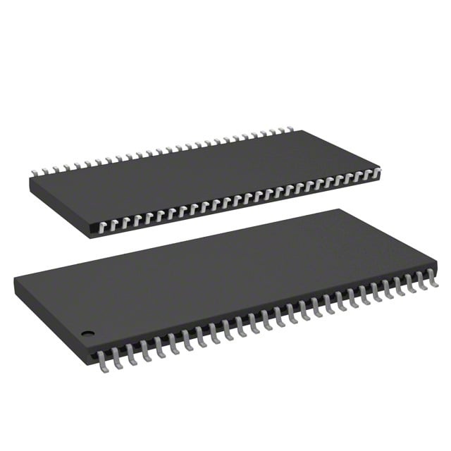
| Device Package | 54-TSOP II | Memory Format | DRAM | Technology | SDRAM | ||
|---|---|---|---|---|---|---|---|
| Memory Size | 128 Mbit | Access Time | 5.4 ns | Grade | Industrial | ||
| Clock Frequency | 143 MHz | Voltage | 3V ~ 3.6V | Memory Type | Volatile | ||
| Operating Temperature | -40°C ~ 85°C (TA) | Write Cycle Time Word Page | N/A | Packaging | 54-TSOP (0.400", 10.16mm Width) | ||
| Mounting Method | Volatile | Memory Interface | Parallel | Memory Organization | 8M x 16 | ||
| Moisture Sensitivity Level | 3 (168 Hours) | RoHS Compliance | ROHS3 Compliant | REACH Compliance | REACH Unaffected | ||
| Qualification | N/A | ECCN | EAR99 | HTS Code | 8542.32.0002 |
Overview of IS45S16800E-7TLA1 – IC DRAM 128MBIT PAR 54TSOP II
The IS45S16800E-7TLA1 is a 128 Mbit synchronous DRAM (SDRAM) device organized as 8M × 16 with a parallel LVTTL interface and quad-bank internal architecture. It implements a pipeline, fully synchronous design with registered inputs and outputs referenced to the rising edge of the clock.
Designed for systems that require compact, board-level SDRAM in a 54-pin TSOP II package, the device offers programmable burst lengths and sequence, selectable CAS latency, and refresh/self-refresh modes to support high-speed data transfer and predictable timing behavior.
Key Features
- Memory Core & Organization 128 Mbit SDRAM organized as 8M × 16 with four internal banks (2M ×16 ×4), supporting random column address every clock cycle for efficient memory access.
- Synchronous Pipeline Architecture Fully synchronous operation with all signals referenced to the positive clock edge and pipeline architecture for high-speed data transfer.
- Performance Operates at up to 143 MHz for the –7 speed grade with an access time from clock of 5.4 ns (CAS latency = 3).
- Programmable Burst & Timing Programmable burst lengths (1, 2, 4, 8, full page) and burst sequence (sequential/interleave); programmable CAS latency options of 2 or 3 clocks.
- Refresh & Power Modes Supports Auto Refresh (CBR) and Self Refresh; 4096 refresh cycles per 16 ms (A2 grade) or 64 ms (A1 grade) as specified in the device options.
- Interface & Logic Levels LVTTL-compatible inputs and outputs with a parallel memory interface suitable for standard SDRAM controller implementations.
- Power Supply Operates at a supply range of 3.0 V to 3.6 V with typical 3.3 V VDD and VDDQ operation.
- Package & Mounting 54-pin TSOP II (0.400", 10.16 mm width) package for compact board-level mounting.
- Operating Temperature Specified operating ambient range of –40 °C to +85 °C (TA) for the provided option.
Typical Applications
- Embedded Systems Board-level SDRAM for embedded designs that require a 128 Mbit parallel memory in a compact 54-TSOP II package.
- Communications Equipment Buffer and working memory in systems where synchronous, clocked data transfer and programmable burst behavior are needed.
- Industrial Control Memory for control and data-logging applications that require operation across an ambient range of –40 °C to +85 °C.
- Consumer Electronics On-board SDRAM for devices needing configurable burst lengths and CAS latency options for diverse throughput requirements.
Unique Advantages
- Synchronous, clocked operation: Performance and timing are driven by a positive-edge clock reference, enabling predictable pipeline data transfers at up to 143 MHz.
- Flexible burst and latency control: Programmable burst lengths/sequences and CAS latency options allow designers to tune throughput and latency to match system requirements.
- Compact TSOP II footprint: 54-pin TSOP II package (10.16 mm width) minimizes board area for space-constrained designs while providing a parallel interface.
- Robust refresh and low-power modes: Auto Refresh and Self Refresh support system-level power management and data retention during low-power states.
- Wide operating voltage window: 3.0 V to 3.6 V supply range with typical 3.3 V operation for compatibility with standard memory power domains.
- Extended ambient temperature range: Specified for –40 °C to +85 °C to support designs exposed to a broad range of operating conditions.
Why Choose IS45S16800E-7TLA1?
The IS45S16800E-7TLA1 provides a compact, fully synchronous 128 Mbit SDRAM solution that balances performance, configurability, and board-level integration. Its programmable burst options, CAS latency selections, and quad-bank architecture make it well suited for designs that require predictable high-speed parallel memory behavior in a space-efficient TSOP II package.
This device is a fit for engineers and procurement teams specifying on-board SDRAM where a defined clocked interface, selectable timing parameters, and operating range down to –40 °C are required. Its features enable tuning of throughput and power characteristics to match system needs while maintaining standard 3.3 V memory system compatibility.
Request a quote or submit an inquiry for pricing and availability to get detailed lead-time and ordering information for the IS45S16800E-7TLA1.