IS45S16800E-7TLA2-TR
| Part Description |
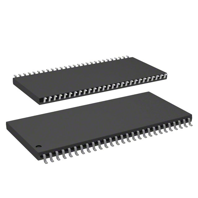
IC DRAM 128MBIT PAR 54TSOP II |
|---|---|
| Quantity | 124 Available (as of June 15, 2026) |

| Product Category | Memory |
|---|---|
| Manufacturer | Integrated Silicon Solution Inc |
| Manufacturing Status | Obsolete |
| Manufacturer Standard Lead Time | Contact Us |
| Datasheet |
Specifications & Environmental
| Device Package | 54-TSOP II | Memory Format | DRAM | Technology | SDRAM | ||
|---|---|---|---|---|---|---|---|
| Memory Size | 128 Mbit | Access Time | 5.4 ns | Grade | Automotive | ||
| Clock Frequency | 143 MHz | Voltage | 3V ~ 3.6V | Memory Type | Volatile | ||
| Operating Temperature | -40°C ~ 105°C (TA) | Write Cycle Time Word Page | N/A | Packaging | 54-TSOP (0.400", 10.16mm Width) | ||
| Mounting Method | Volatile | Memory Interface | Parallel | Memory Organization | 8M x 16 | ||
| Moisture Sensitivity Level | 3 (168 Hours) | RoHS Compliance | ROHS3 Compliant | REACH Compliance | REACH Unaffected | ||
| Qualification | N/A | ECCN | EAR99 | HTS Code | 8542.32.0002 |
Overview of IS45S16800E-7TLA2-TR – 128Mbit SDRAM, 54‑TSOP II, 143 MHz
The IS45S16800E-7TLA2-TR is a 128Mbit synchronous DRAM (SDRAM) device organized as 8M × 16 with a quad-bank architecture and a fully synchronous, pipelined interface. It is designed for high-speed data transfer with all signals referenced to the rising edge of the clock and an LVTTL-compatible interface.
This SDRAM suits designs that require predictable, high-throughput parallel memory—providing programmable burst lengths and CAS latencies, internal bank management for row access/precharge hiding, and on-chip refresh mechanisms to support continuous operation across a broad temperature range.
Key Features
- Memory Core 128Mbit SDRAM organized as 8M × 16 bits across four internal banks, enabling concurrent bank operation and efficient row management.
- Performance & Timing Operates up to 143 MHz (‑7 speed grade) with an access time from clock of 5.4 ns (CAS latency = 3). Programmable CAS latency options include 2 and 3 clocks.
- Burst & Sequencing Programmable burst lengths (1, 2, 4, 8, full page) and selectable sequential or interleave burst sequences for flexible data transfer patterns.
- Refresh & Power Modes Supports auto refresh (CBR) and self refresh; device offers 4096 refresh cycles per interval depending on grade. Includes power-saving power-down and self-refresh capabilities.
- Interface Parallel LVTTL-compatible interface with random column address capability every clock cycle for predictable column accesses.
- Voltage & Supply Designed for 3.3 V operation; documented operating supply range includes 3.0 V to 3.6 V.
- Temperature Range Specified for operation from −40°C to +105°C (TA) for the high-temperature option.
- Package 54-pin TSOP II package (0.400", 10.16 mm width) for compact board-level footprint and standard surface-mount assembly.
Typical Applications
- High-speed buffering Parallel SDRAM buffering where predictable synchronous timing and programmable burst transfers are required.
- Embedded system memory System memory expansion in designs that need 128 Mbit of volatile SDRAM with a parallel LVTTL interface.
- Data capture and frame storage Temporary storage for streaming data where internal bank interleaving and burst modes improve throughput.
Unique Advantages
- Deterministic synchronous operation: All signals referenced to the rising edge of the clock, enabling tight timing control and predictable data transfers.
- High-throughput capability: 143 MHz clock operation with 5.4 ns access from clock at CAS = 3 supports fast read/write cycles.
- Flexible data handling: Programmable burst lengths and burst sequencing allow tuning for sequential or interleaved access patterns.
- Built-in refresh and power modes: Auto refresh and self-refresh plus power-down reduce external management and support low-power idle states.
- Wide operating temperature: Specified operation from −40°C to +105°C supports deployment in temperature-challenging environments.
- Standard TSOP II footprint: 54-pin TSOP II package provides a compact, industry-standard surface-mount option for board-level integration.
Why Choose IS45S16800E-7TLA2-TR?
The IS45S16800E-7TLA2-TR combines a synchronous, pipelined SDRAM architecture with programmable timing and burst options to give designers deterministic performance and flexible data-transfer modes. Its 8M × 16 organization and quad-bank structure enable efficient row management and concurrent operations suited to high-throughput parallel memory requirements.
This device is appropriate for engineers and procurement teams seeking a 128 Mbit SDRAM in a compact 54‑pin TSOP II package with documented timing (143 MHz, 5.4 ns access), LVTTL interface compatibility, on-chip refresh support, and a broad operating temperature range for robust system-level deployment.
Request a quote or submit an inquiry to obtain pricing, availability, and lead-time information for the IS45S16800E-7TLA2-TR.