IS45S16800E-7BLA2-TR
| Part Description |
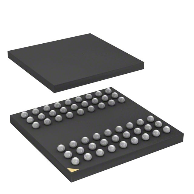
IC DRAM 128MBIT PAR 54TFBGA |
|---|---|
| Quantity | 1,119 Available (as of June 15, 2026) |

| Product Category | Memory |
|---|---|
| Manufacturer | Integrated Silicon Solution Inc |
| Manufacturing Status | Obsolete |
| Manufacturer Standard Lead Time | Contact Us |
| Datasheet |
Specifications & Environmental
| Device Package | 54-TFBGA (8x8) | Memory Format | DRAM | Technology | SDRAM | ||
|---|---|---|---|---|---|---|---|
| Memory Size | 128 Mbit | Access Time | 5.4 ns | Grade | Automotive | ||
| Clock Frequency | 143 MHz | Voltage | 3V ~ 3.6V | Memory Type | Volatile | ||
| Operating Temperature | -40°C ~ 105°C (TA) | Write Cycle Time Word Page | N/A | Packaging | 54-TFBGA | ||
| Mounting Method | Volatile | Memory Interface | Parallel | Memory Organization | 8M x 16 | ||
| Moisture Sensitivity Level | 3 (168 Hours) | RoHS Compliance | ROHS3 Compliant | REACH Compliance | REACH Unaffected | ||
| Qualification | N/A | ECCN | EAR99 | HTS Code | 8542.32.0002 |
Overview of IS45S16800E-7BLA2-TR – 128 Mbit SDRAM, 54‑TFBGA, Parallel Interface
The IS45S16800E-7BLA2-TR is a 128 Mbit synchronous DRAM (SDRAM) organized as 8M × 16 with an internal quad-bank architecture and fully synchronous, pipelined operation. It provides parallel memory access with LVTTL-compatible signaling and programmable burst operations for high-throughput data transfers.
This device targets designs that require a 128 Mbit parallel SDRAM solution operating from a 3.0 V–3.6 V supply and packaged in a compact 54‑TFBGA (8×8) footprint. Key value propositions include deterministic clocked operation, selectable CAS latency and burst control, and extended operating temperature support.
Key Features
- Memory Architecture Organized as 8M × 16 (128 Mbit) with an internal quad-bank DRAM structure and 4,096 rows by 512 columns by 16 bits per bank, enabling banked accesses and pipeline efficiency.
- High‑Speed Operation Clock frequency supported at 143 MHz (-7 device) with an access time from clock of 5.4 ns at CAS latency = 3, enabling fast synchronous reads and writes.
- Synchronous Interface & Timing Fully synchronous device with all signals referenced to the rising edge of CLK, LVTTL input/output levels, programmable CAS latency (2 or 3 clocks), and programmable burst lengths (1, 2, 4, 8, full page).
- Burst and Refresh Control Programmable burst sequence (sequential/interleave), burst termination by burst stop and precharge commands, Auto Refresh and Self Refresh modes with 4,096 refresh cycles per specified refresh interval (A2: 16 ms or A1: 64 ms variants documented).
- Power and Supply Designed for operation with a 3.0 V to 3.6 V supply range (device datasheet references 3.3 V VDD/VDDQ), and includes power-saving modes such as self-refresh and power-down.
- Package and Thermal Supplied in a 54‑TFBGA (8×8) ball grid array package; operating ambient temperature range of -40°C to +105°C (TA) for the A2 option.
Typical Applications
- Embedded systems requiring parallel SDRAM Use as off-chip system memory where a 128 Mbit parallel SDRAM with LVTTL interface and programmable burst control is required.
- High-speed buffering and data capture 128 Mbit density with programmable burst lengths and 143 MHz clock capability supports high-throughput buffering and burst transfers.
- Memory expansion for processing modules Provides parallel SDRAM capacity for modules that need 16-bit data paths and synchronous, pipelined access.
Unique Advantages
- Synchronous, pipelined operation: Enables predictable timing and aligns all signals to the rising edge of CLK for deterministic performance in clocked systems.
- Flexible burst control: Programmable burst lengths and sequence modes (sequential/interleave) allow matching access patterns to system requirements and optimizing throughput.
- Selectable CAS latency: CAS latency options (2 or 3) and documented timing (5.4 ns access at CL=3) provide tuning for trade-offs between speed and timing margins.
- Power management features: Auto Refresh, Self Refresh and power-down modes support lower-power operation during idle periods.
- Wide operating temperature: Specified -40°C to +105°C (TA) for the A2 option to support designs requiring extended ambient temperature range.
- Compact BGA package: 54‑TFBGA (8×8) footprint reduces board area for dense layouts while providing necessary ballout for parallel interfaces.
Why Choose IC DRAM 128MBIT PAR 54TFBGA?
The IS45S16800E-7BLA2-TR combines a 128 Mbit density, quad-bank SDRAM architecture and fully synchronous LVTTL interface to deliver a deterministic, high-throughput parallel memory option. Its programmable burst behavior, selectable CAS latency, and documented timing (143 MHz, 5.4 ns access at CL=3) let engineers tune performance to match system timing and throughput requirements.
This device suits designs that need a compact 54‑TFBGA package, a 3.0 V–3.6 V supply envelope, and extended ambient temperature capability up to +105°C (TA option A2). It offers a balance of performance, timing flexibility, and power management features appropriate for embedded memory expansion and high-speed buffering tasks.
Request a quote or submit a request for pricing and availability for the IS45S16800E-7BLA2-TR to evaluate fit for your design and production needs.