IS45S16800E-7BLA2
| Part Description |
IC DRAM 128MBIT PAR 54TFBGA |
|---|---|
| Quantity | 562 Available (as of June 15, 2026) |

| Product Category | Memory |
|---|---|
| Manufacturer | Integrated Silicon Solution Inc |
| Manufacturing Status | Obsolete |
| Manufacturer Standard Lead Time | Contact Us |
| Datasheet |
Specifications & Environmental
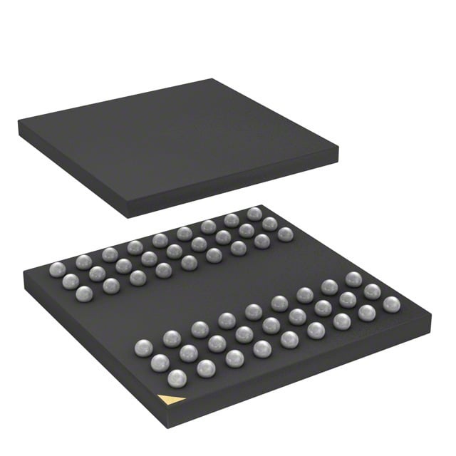
| Device Package | 54-TFBGA (8x8) | Memory Format | DRAM | Technology | SDRAM | ||
|---|---|---|---|---|---|---|---|
| Memory Size | 128 Mbit | Access Time | 5.4 ns | Grade | Automotive | ||
| Clock Frequency | 143 MHz | Voltage | 3V ~ 3.6V | Memory Type | Volatile | ||
| Operating Temperature | -40°C ~ 105°C (TA) | Write Cycle Time Word Page | N/A | Packaging | 54-TFBGA | ||
| Mounting Method | Volatile | Memory Interface | Parallel | Memory Organization | 8M x 16 | ||
| Moisture Sensitivity Level | 3 (168 Hours) | RoHS Compliance | ROHS3 Compliant | REACH Compliance | REACH Unaffected | ||
| Qualification | N/A | ECCN | EAR99 | HTS Code | 8542.32.0002 |
Overview of IS45S16800E-7BLA2 – IC DRAM 128MBIT PAR 54TFBGA
The IS45S16800E-7BLA2 is a 128 Mbit synchronous DRAM (SDRAM) organized as 8M × 16 with a fully synchronous, pipelined architecture. It provides parallel memory access with programmable burst operation and CAS latency options for deterministic, clock-referenced data transfers.
Designed for systems that require a compact, high-speed volatile memory device, this SDRAM offers selectable performance modes, internal bank architecture for row access/precharge hiding, and a compact 54-ball TFBGA package suitable for space-constrained boards.
Key Features
- Core & Architecture Quad-bank SDRAM with pipelined operation; all inputs and outputs are referenced to the rising edge of the clock for fully synchronous operation.
- Memory Capacity & Organization 128 Mbit total capacity, organized as 8M × 16 bits (2,048K words × 16) to support parallel data paths.
- Performance -7 speed grade with 143 MHz clock frequency and 5.4 ns access time (CAS latency = 3). Programmable CAS latency options of 2 or 3 clocks.
- Burst & Sequencing Programmable burst length (1, 2, 4, 8, full page) and selectable burst sequence (sequential or interleave) for flexible transfer patterns.
- Refresh & Power Management Auto Refresh (CBR) and Self Refresh support with specified refresh cycles (4096 cycles per refresh window dependent on grade) to maintain data integrity in volatile operation.
- Interface Parallel memory interface with LVTTL-compatible signals and random column address every clock cycle for efficient read/write access.
- Voltage & Supply VDD / VDDQ nominal 3.3 V with an operating supply range of 3.0 V to 3.6 V.
- Package & Mounting 54-ball TFBGA (8 × 8) compact package for surface-mount assembly.
- Operating Temperature Extended ambient temperature range from −40°C to +105°C (TA) for temperature-tolerant applications.
Typical Applications
- High-speed system memory Use where a fully synchronous SDRAM with 143 MHz operation and programmable CAS latency is required for deterministic data transfers.
- Embedded and industrial systems Suited to boards operating across a wide ambient temperature range (−40°C to +105°C), providing reliable volatile storage in industrial environments.
- Memory subsystems and buffering Programmable burst lengths and internal bank architecture make the device appropriate for parallel buffering and burst-oriented transfer patterns.
Unique Advantages
- Deterministic synchronous interface: All signals referenced to the positive clock edge for predictable timing across system designs.
- Flexible performance scaling: Selectable CAS latency (2 or 3) and multiple burst lengths enable trade-offs between throughput and latency.
- Efficient bank architecture: Internal quad-bank design hides row access/precharge latencies to improve effective throughput for burst accesses.
- Wide operating temperature: −40°C to +105°C rating supports deployment in thermally demanding environments.
- Compact BGA footprint: 54-ball TFBGA (8×8) reduces board area for space-constrained applications.
Why Choose IS45S16800E-7BLA2?
The IS45S16800E-7BLA2 combines a 128 Mbit SDRAM organization with a fully synchronous, pipelined architecture and programmable timing to deliver predictable, high-speed parallel memory operation. Its selectable CAS latency, burst control, and internal bank structure provide designers with configurable performance options to match system requirements.
With a 3.0 V–3.6 V supply range, LVTTL interface, and a compact 54-ball TFBGA package rated for −40°C to +105°C, this device is well suited to designs that need a compact, temperature-tolerant volatile memory solution with flexible timing and burst capabilities.
Request a quote or submit an inquiry for IS45S16800E-7BLA2 to receive pricing and lead-time information tailored to your procurement needs.