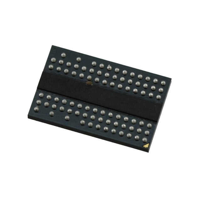
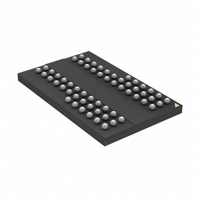
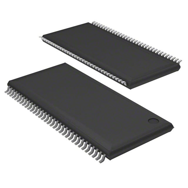
IS46R16160D-5TLA1
| Part Description |
IC DRAM 256MBIT PAR 66TSOP II |
|---|---|
| Quantity | 1,517 Available (as of June 15, 2026) |
| Product Category | Memory |
|---|---|
| Manufacturer | Integrated Silicon Solution Inc |
| Manufacturing Status | Obsolete |
| Manufacturer Standard Lead Time | Contact Us |
| Datasheet |
Specifications & Environmental
| Device Package | 66-TSOP II | Memory Format | DRAM | Technology | SDRAM - DDR | ||
|---|---|---|---|---|---|---|---|
| Memory Size | 256 Mbit | Access Time | 700 ps | Grade | Industrial | ||
| Clock Frequency | 200 MHz | Voltage | 2.3V ~ 2.7V | Memory Type | Volatile | ||
| Operating Temperature | -40°C ~ 85°C (TA) | Write Cycle Time Word Page | 15 ns | Packaging | 66-TSSOP (0.400", 10.16mm Width) | ||
| Mounting Method | Volatile | Memory Interface | Parallel | Memory Organization | 16M x 16 | ||
| Moisture Sensitivity Level | 3 (168 Hours) | RoHS Compliance | ROHS3 Compliant | REACH Compliance | REACH Unaffected | ||
| Qualification | N/A | ECCN | EAR99 | HTS Code | 8542.32.0024 |
Overview of IS46R16160D-5TLA1 – IC DRAM 256MBIT PAR 66TSOP II
The IS46R16160D-5TLA1 is a 256Mbit DDR SDRAM device organized as 16M × 16 with a parallel memory interface. It implements a double-data-rate pipeline architecture with internal banked memory to deliver continuous burst reads and writes and high-throughput data transfer.
Designed for systems requiring compact, low-voltage DDR memory, this device offers a 66‑pin TSOP‑II package, programmable latency and burst options, and an industrial operating range to support robust embedded and electronic designs.
Key Features
- Memory Core and Organization 256Mbit DDR SDRAM organized as 16M × 16 with four internal banks to support concurrent operations and burst accesses.
- Double-Data-Rate Architecture Two data transfers per clock cycle with data strobe (DQS) transmitted/received with data; DQS edge-aligned for READs and centre-aligned for WRITEs.
- Performance Maximum clock frequency up to 200 MHz (speed grade -5) with an access time of 700 ps and a word page write cycle time of 15 ns for high-rate burst transfers.
- Programmability and Burst Control Burst lengths of 2, 4 and 8, selectable burst type (sequential or interleave) and programmable CAS latency options (2, 2.5 and 3) to match system timing requirements.
- Clocking and Timing Differential clock inputs (CK and CK̄) with internal DLL to align DQ/DQS transitions to clock edges; commands registered on positive CK edge and data referenced to both edges of DQS.
- Interface Compatibility SSTL_2 compatible I/O and data mask (DM) that masks write data on both rising and falling edges of the data strobe.
- Power VDD and VDDQ at 2.5V ±0.2V (specified supply range 2.3V–2.7V) for low-voltage operation.
- Refresh and Reliability Supports Auto Refresh and Self Refresh modes plus Auto Precharge; TRAS Lockout supported (tRAP = tRCD) to manage row timing.
- Package and Temperature 66‑TSSOP (66‑TSOP II) package (0.400", 10.16 mm width) and specified operating temperature range of −40°C to +85°C (TA).
Typical Applications
- Embedded systems Provides a compact 256Mbit DDR memory option for embedded designs requiring parallel DDR SDRAM in a 66‑TSOP II footprint.
- Consumer and industrial electronics Suitable for electronic modules that need low-voltage DDR SDRAM with programmable latency and burst modes to match system timing.
- Memory expansion in compact boards Fits board-level memory expansion where a 16M × 16 parallel DDR device in a small TSOP‑II package is required.
Unique Advantages
- Dual-data-rate throughput: Double-data-rate architecture enables two data transfers per clock cycle for higher effective bandwidth.
- Flexible timing configuration: Programmable CAS latencies (2, 2.5, 3) and selectable burst lengths (2/4/8) allow tuning to system performance and latency needs.
- Low-voltage operation: Specified VDD/VDDQ at 2.5V ±0.2V (supply range 2.3–2.7V) reduces overall power compared with higher-voltage memories.
- Compact package: 66‑TSOP II package (10.16 mm width) provides a small-footprint option for space-constrained PCBs.
- Robust timing and refresh features: DLL alignment, data strobe handling (DQS), Auto/Self Refresh and Auto Precharge support reliable data integrity in continuous burst operation.
- Banked architecture: Four internal banks enable concurrent operations to improve effective throughput for burst and pipelined accesses.
Why Choose IS46R16160D-5TLA1?
The IS46R16160D-5TLA1 combines DDR SDRAM performance with flexible timing and burst control in a compact 66‑TSOP II package. Its 16M × 16 organization, support for programmable CAS latency and multiple burst lengths, plus SSTL_2 I/O compatibility, make it suitable for designs that require adaptable, high-throughput parallel memory at low voltage.
This device is well suited to engineers and procurement teams specifying board-level DDR memory for embedded and electronic systems where package size, operating temperature (−40°C to +85°C) and configurable timing are key considerations.
Request a quote or submit an inquiry for pricing and availability of the IS46R16160D-5TLA1 to receive product lead-time and bulk pricing information.