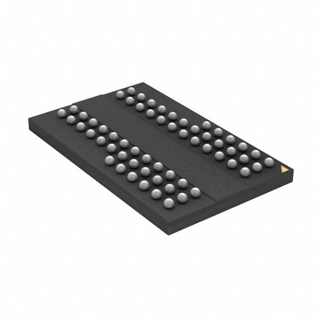
IS46R16160D-6BLA2
| Part Description |
IC DRAM 256MBIT PAR 60TFBGA |
|---|---|
| Quantity | 1,381 Available (as of June 15, 2026) |

| Product Category | Memory |
|---|---|
| Manufacturer | Integrated Silicon Solution Inc |
| Manufacturing Status | Obsolete |
| Manufacturer Standard Lead Time | Contact Us |
| Datasheet |
Specifications & Environmental
| Device Package | 60-TFBGA (8x13) | Memory Format | DRAM | Technology | SDRAM - DDR | ||
|---|---|---|---|---|---|---|---|
| Memory Size | 256 Mbit | Access Time | 700 ps | Grade | Automotive | ||
| Clock Frequency | 166 MHz | Voltage | 2.3V ~ 2.7V | Memory Type | Volatile | ||
| Operating Temperature | -40°C ~ 105°C (TA) | Write Cycle Time Word Page | 15 ns | Packaging | 60-TFBGA | ||
| Mounting Method | Volatile | Memory Interface | Parallel | Memory Organization | 16M x 16 | ||
| Moisture Sensitivity Level | 3 (168 Hours) | RoHS Compliance | ROHS3 Compliant | REACH Compliance | REACH Unaffected | ||
| Qualification | N/A | ECCN | EAR99 | HTS Code | 8542.32.0024 |
Overview of IS46R16160D-6BLA2 – 256Mbit DDR SDRAM, 60-TFBGA
The IS46R16160D-6BLA2 is a 256 Mbit DDR SDRAM organized as 16M × 16 bits in a 60-ball TFBGA (8×13) package. It implements a double-data-rate architecture with on-die DLL and data strobe (DQS) timing to support high-speed bidirectional data transfers referenced to both clock and DQS edges.
Designed for systems that require parallel DDR memory in a compact BGA footprint, this device provides selectable burst lengths, programmable CAS latency and standard refresh modes to support continuous read/write burst operation and flexible timing control.
Key Features
- Core / Memory Organization 256 Mbit capacity organized as 16M × 16 with four internal banks to enable concurrent bank operations and continuous burst access.
- DDR Architecture Double-data-rate operation with two data transfers per clock cycle; DQS is transmitted/received with data and is edge-aligned for READs and centre-aligned for WRITEs.
- Timing and Latency Programmable CAS latency options (2, 2.5 and 3) and burst lengths of 2, 4 and 8; commands are registered on the positive edge of CLK and data/masks are referenced to DQS edges.
- Interface and Signalling SSTL_2-compatible I/O, differential clock inputs (CK and CK̄) and Data Mask (DM) for masking write data on both DQS edges.
- Power VDD and VDDQ nominal 2.5 V (±0.2 V); supply operating range listed as 2.3 V to 2.7 V in the product specification.
- Performance Clock frequency rating around 166 MHz for the -6 speed grade and access timing characteristics including 700 ps access time and 15 ns write cycle time (word page).
- Refresh and Reliability Supports Auto Refresh and Self Refresh modes, Auto Precharge and TRAS lockout (tRAP = tRCD) for standard DRAM maintenance and timing control.
- Package and Temperature 60-TFBGA (8×13) ball BGA package; operating temperature range specified as –40°C to +105°C (TA).
Typical Applications
- DDR memory subsystems — Used as parallel DDR SDRAM in systems requiring 256 Mbit of DDR memory with programmable latency and burst control.
- Compact board-level designs — 60-ball TFBGA (8×13) package suits space-constrained PCBs that require high-density parallel memory.
- High-rate data buffering — Double-data-rate architecture and DQS-aligned transfers support continuous read/write burst operation for buffering tasks.
Unique Advantages
- DDR double-data-rate transfers — Two data transfers per clock cycle increase effective bandwidth compared to single-rate memories without changing clock speed.
- Flexible timing configuration — Programmable CAS latencies (2, 2.5, 3) and multiple burst lengths (2, 4, 8) enable tuning for system timing and throughput requirements.
- SSTL_2-compatible I/O and differential clocking — Industry-standard signaling options simplify integration into SSTL_2-capable interfaces and systems using differential clocks.
- Robust refresh and power modes — Auto Refresh and Self Refresh modes plus Auto Precharge and TRAS lockout provide standard DRAM maintenance for reliable operation.
- Wide supply and temperature windows — Supply range of 2.3 V–2.7 V with an operating temperature of –40°C to +105°C supports a range of board- and environment-level requirements.
- Compact BGA footprint — 60-TFBGA (8×13) package delivers 256 Mbit density in a compact form factor for space-limited designs.
Why Choose IS46R16160D-6BLA2?
The IS46R16160D-6BLA2 combines DDR SDRAM architecture, SSTL_2-compatible I/O and programmable timing to provide a compact, configurable 256 Mbit memory building block for systems that require parallel DDR performance in a small BGA package. Its supported refresh modes, selectable CAS latency and burst options make it suitable for designs that need predictable burst transfers and timing flexibility.
This device is appropriate for engineers and procurement teams specifying board-level DDR memory where supply voltage range, package density and operating temperature window are primary selection criteria. The IS46R16160D-6BLA2 offers clear, datasheet-defined electrical and timing characteristics to support integration and system-level validation.
Request a quote or submit an inquiry to receive pricing, lead-time and availability information for the IS46R16160D-6BLA2. Our team can provide the details you need to evaluate this DDR SDRAM for your design.