IS46R16160D-6TLA2
| Part Description |
IC DRAM 256MBIT PAR 66TSOP II |
|---|---|
| Quantity | 1,271 Available (as of June 11, 2026) |
| Product Category | Memory |
|---|---|
| Manufacturer | Integrated Silicon Solution Inc |
| Manufacturing Status | Obsolete |
| Manufacturer Standard Lead Time | Contact Us |
| Datasheet |
Specifications & Environmental
| Device Package | 66-TSOP II | Memory Format | DRAM | Technology | SDRAM - DDR | ||
|---|---|---|---|---|---|---|---|
| Memory Size | 256 Mbit | Access Time | 700 ps | Grade | Automotive | ||
| Clock Frequency | 166 MHz | Voltage | 2.3V ~ 2.7V | Memory Type | Volatile | ||
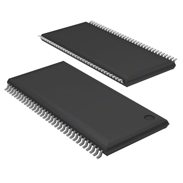
| Operating Temperature | -40°C ~ 105°C (TA) | Write Cycle Time Word Page | 15 ns | Packaging | 66-TSSOP (0.400", 10.16mm Width) | ||
| Mounting Method | Volatile | Memory Interface | Parallel | Memory Organization | 16M x 16 | ||
| Moisture Sensitivity Level | 3 (168 Hours) | RoHS Compliance | ROHS3 Compliant | REACH Compliance | REACH Unaffected | ||
| Qualification | N/A | ECCN | EAR99 | HTS Code | 8542.32.0024 |
Overview of IS46R16160D-6TLA2 – IC DRAM 256MBIT PAR 66TSOP II
The IS46R16160D-6TLA2 is a 256 Mbit DDR SDRAM device organized as 16M × 16 with a parallel memory interface in a 66‑pin TSOP‑II package. It implements a double‑data‑rate architecture with pipeline operation and four internal banks to support continuous read/write burst transfers.
Its feature set — including SSTL_2‑compatible I/O, programmable CAS latency, and support for burst lengths of 2, 4 and 8 — targets designs that require a mid‑density parallel DDR memory solution with configurable timing and compact packaging.
Key Features
- Memory Core 256 Mbit DRAM organized as 16M × 16 with four internal banks for concurrent operation and pipeline access.
- DDR Architecture Double‑data‑rate operation with two data transfers per clock cycle and data strobe (DQS) transmitted/received for read/write capture.
- Timing and Performance Support for programmable CAS latency (2, 2.5, 3), burst lengths 2/4/8, and burst type sequential or interleave; typical clock frequency listed at 166 MHz and access time 700 ps.
- Interface and Signaling SSTL_2 compatible I/O, differential clock inputs (CK and ÌCK), DLL alignment of DQ/DQS with clock, and data mask (DM) for write masking at both edges of DQS.
- Power VDD and VDDQ specified at 2.5 V ± 0.2 V with supply operating range 2.3 V to 2.7 V.
- Refresh and Power Modes Auto Refresh and Self Refresh modes supported; Auto Precharge and TRAS lockout (tRAP = tRCD) provided.
- Package & Temperature 66‑pin TSOP‑II package (0.400", 10.16 mm width) with operating ambient temperature range −40 °C to +105 °C (TA).
- Write and Cycle Timing Write cycle time (word/page) of 15 ns and timing parameters compliant with device speed grades.
Typical Applications
- Embedded memory subsystems Provides mid‑density parallel DDR storage for systems that require a 256 Mbit volatile memory block with configurable latency and burst behavior.
- Board‑level memory expansion Used as on‑board DRAM where SSTL_2 signaling and a compact 66‑TSOP‑II footprint are required to fit space‑constrained PCB layouts.
- Performance‑tuned designs Suitable for designs that leverage programmable CAS latency, burst length and DLL timing to optimize read/write throughput.
Unique Advantages
- Double‑data‑rate throughput: Two data transfers per clock cycle increase effective bandwidth without changing clock rate.
- Flexible timing control: Programmable CAS latency (2, 2.5, 3) and selectable burst lengths (2, 4, 8) let designers tune latency and burst behavior to system needs.
- SSTL_2‑compatible I/O: Standard signaling compatibility simplifies integration with SSTL_2 host interfaces.
- Compact package: 66‑pin TSOP‑II (10.16 mm width) delivers a smaller board footprint for space‑constrained applications.
- Wide operating range: Supply range of 2.3 V to 2.7 V and ambient operation from −40 °C to +105 °C support varied environmental conditions.
- Concurrent bank operation: Four internal banks and pipeline architecture enable near‑continuous burst read/write sequences for sustained data movement.
Why Choose IS46R16160D-6TLA2?
The IS46R16160D-6TLA2 delivers a focused combination of DDR performance, selectable timing options and a compact TSOP‑II package for designs that need a 256 Mbit parallel DRAM solution. Its SSTL_2 signaling, DLL timing alignment and support for multiple burst/latency modes make it suitable for systems where predictable timing and integration with standard DDR hosts are important.
This device is aimed at engineers specifying a mid‑density, configurable DDR SDRAM for board‑level memory subsystems that require a well‑documented timing feature set, compact package, and an extended ambient operating range.
Request a quote or submit an inquiry to discuss availability, lead times and pricing for the IS46R16160D-6TLA2.