IS46R16160D-6BLA1-TR
| Part Description |
IC DRAM 256MBIT PAR 60TFBGA |
|---|---|
| Quantity | 938 Available (as of June 15, 2026) |
| Product Category | Memory |
|---|---|
| Manufacturer | Integrated Silicon Solution Inc |
| Manufacturing Status | Obsolete |
| Manufacturer Standard Lead Time | Contact Us |
| Datasheet |
Specifications & Environmental
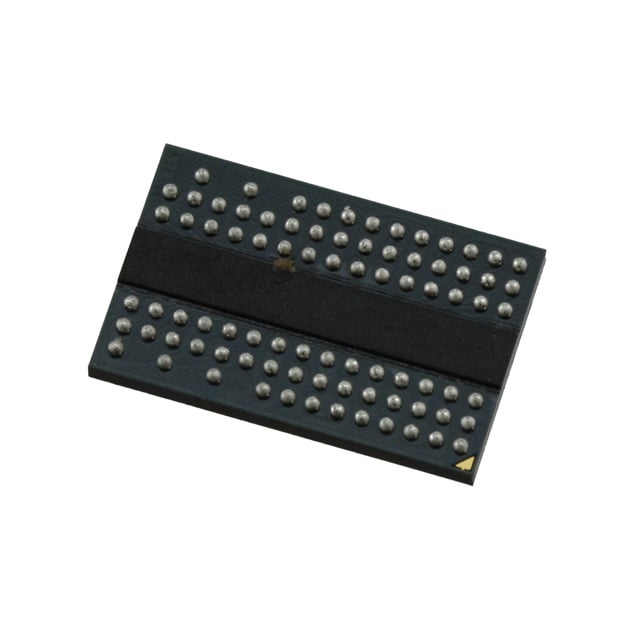
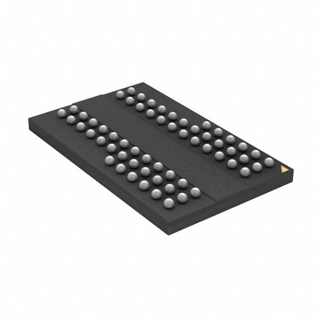
| Device Package | 60-TFBGA (8x13) | Memory Format | DRAM | Technology | SDRAM - DDR | ||
|---|---|---|---|---|---|---|---|
| Memory Size | 256 Mbit | Access Time | 700 ps | Grade | Industrial | ||
| Clock Frequency | 166 MHz | Voltage | 2.3V ~ 2.7V | Memory Type | Volatile | ||
| Operating Temperature | -40°C ~ 85°C (TA) | Write Cycle Time Word Page | 15 ns | Packaging | 60-TFBGA | ||
| Mounting Method | Volatile | Memory Interface | Parallel | Memory Organization | 16M x 16 | ||
| Moisture Sensitivity Level | 3 (168 Hours) | RoHS Compliance | ROHS3 Compliant | REACH Compliance | REACH Unaffected | ||
| Qualification | N/A | ECCN | EAR99 | HTS Code | 8542.32.0024 |
Overview of IS46R16160D-6BLA1-TR – IC DRAM 256MBIT PAR 60TFBGA
The IS46R16160D-6BLA1-TR is a 256 Mbit DDR SDRAM organized as 16M × 16 with a parallel memory interface in a 60‑TFBGA (8×13) package. It implements a double-data-rate architecture with bidirectional data strobe (DQS) and an internal DLL to align data and clock transitions for high-speed burst transfers.
This device targets systems requiring compact, high-speed volatile memory with programmable burst length and CAS latency options, offering a clock frequency rating up to 166 MHz and an operating temperature range of -40°C to 85°C.
Key Features
- Core / Architecture Double‑data‑rate (DDR) SDRAM with four internal banks and pipeline architecture to support continuous read/write burst accesses.
- Memory Organization & Capacity 256 Mbit capacity organized as 16M × 16, suitable for 16‑bit data bus implementations.
- Performance Rated clock frequency up to 166 MHz with programmable CAS latency options (2, 2.5, 3) and burst lengths of 2, 4 and 8.
- Data Timing & Signaling Bidirectional DQS transmitted/received with data (edge‑aligned for reads, center‑aligned for writes); DLL aligns DQ and DQS transitions with CK; differential clock inputs (CK/CK̅).
- Interface Compatibility SSTL_2 compatible I/O and parallel memory interface for integration with SSTL_2 signalling systems.
- Power VDD and VDDQ supply range 2.3 V to 2.7 V (2.5 V ±0.2 V specified).
- Timing Write cycle time (word page) 15 ns and access time listed at 700 ps in the product specification.
- Package & Temperature 60‑ball TFBGA (8×13) supplier device package with operating temperature range of -40°C to 85°C (TA).
Typical Applications
- High‑speed memory subsystems Devices and modules that require DDR SDRAM with 16‑bit organization and configurable burst/CAS timing.
- Embedded systems Compact board‑level designs needing a 256 Mbit volatile memory in a 60‑TFBGA footprint and SSTL_2 I/O signaling.
- Data buffering and burst storage Use cases that benefit from DDR burst transfers and internal banked architecture for concurrent operations.
Unique Advantages
- Double‑data‑rate throughput: Two data transfers per clock cycle deliver higher effective bandwidth compared to single‑edge SDRAM at the same clock frequency.
- Flexible timing configuration: Programmable CAS latencies (2, 2.5, 3) and selectable burst lengths (2/4/8) allow tuning for system latency and bandwidth tradeoffs.
- SSTL_2 I/O compatibility: I/O signaling that matches SSTL_2 standards simplifies interface design with compatible memory controllers.
- Compact BGA package: 60‑TFBGA (8×13) provides a small board footprint for space‑constrained applications.
- Industrial temperature range: Rated for -40°C to 85°C (TA), supporting deployment across a wide range of environmental conditions.
Why Choose IS46R16160D-6BLA1-TR?
The IS46R16160D-6BLA1-TR combines a 256 Mbit DDR SDRAM architecture with flexible timing, SSTL_2 compatible I/O, and a compact 60‑TFBGA package to address designs that require reliable high‑speed volatile memory in constrained form factors. Its programmable CAS latency, multiple burst lengths, and internal DLL/DQS timing support make it suitable where adjustable latency and efficient burst transfers are required.
This part is appropriate for engineering teams designing board‑level memory subsystems that need documented electrical and timing characteristics (VDD/VDDQ supply range, clock frequency rating, access and cycle timing) and a small BGA footprint for integration into embedded or system‑level products.
Request a quote or submit an inquiry to receive pricing and availability information for the IS46R16160D-6BLA1-TR.