MT28F128J3FS-12 ET TR
| Part Description |
IC FLASH 128MBIT PARALLEL 64FBGA |
|---|---|
| Quantity | 536 Available (as of June 15, 2026) |
| Product Category | Flash Memory |
|---|---|
| Manufacturer | Micron Technology Inc. |
| Manufacturing Status | Obsolete |
| Manufacturer Standard Lead Time | Contact Us |
| Datasheet |
Specifications & Environmental
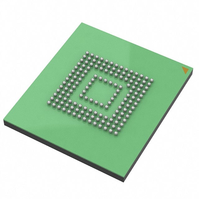
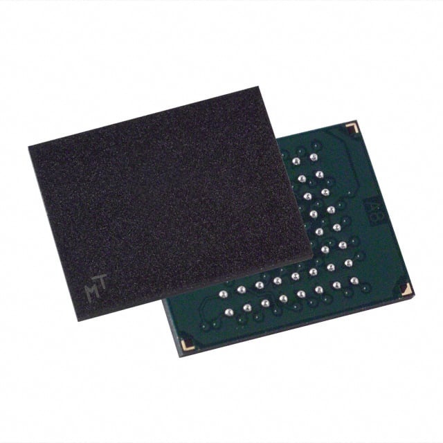
| Device Package | 64-FBGA (10x13) | Memory Format | FLASH | Technology | FLASH | ||
|---|---|---|---|---|---|---|---|
| Memory Size | 128 Mbit | Access Time | 120 ns | Grade | Industrial | ||
| Clock Frequency | N/A | Voltage | 2.7V ~ 3.6V | Memory Type | Non-Volatile | ||
| Operating Temperature | -40°C ~ 85°C (TA) | Write Cycle Time Word Page | N/A | Packaging | 64-FBGA | ||
| Mounting Method | Non-Volatile | Memory Interface | Parallel | Memory Organization | 16M x 8, 8M x 16 | ||
| Moisture Sensitivity Level | 3 (168 Hours) | RoHS Compliance | RoHS non-compliant | REACH Compliance | REACH Unaffected | ||
| Qualification | N/A | ECCN | 3A991B1A | HTS Code | 8542.32.0071 |
Overview of MT28F128J3FS-12 ET TR – IC FLASH 128MBIT PARALLEL 64FBGA
The MT28F128J3FS-12 ET TR is a 128Mbit Q-FLASH® non-volatile parallel FLASH memory device offered in a 64-ball FBGA (10×13) package. It provides x8/x16 memory organization options (16M × 8, 8M × 16) and supports asynchronous page-mode reads.
Targeted at systems requiring parallel NOR-style FLASH storage, the device operates from 2.7 V to 3.6 V and is specified for an operating temperature range of −40°C to +85°C. Key functional strengths include page-mode read performance, configurable protection features, automatic write/erase algorithms and a hardware-friendly industry-standard pinout.
Key Features
- Memory Capacity & Organization — 128 Mbit total memory with x8/x16 organizations: 16M × 8 and 8M × 16 arrangements to match parallel bus requirements.
- Read Performance — Asynchronous page-mode reads with specified access times for the 128Mb device at 120 ns/25 ns (read access time/page cycle value as documented).
- Voltage Range — VCC, VCCQ and VPEN operate across 2.7 V to 3.6 V, including application programming at the same supply range.
- Robust Package & Mounting — 64-ball FBGA (1.00 mm pitch, 10×13) supplier device package suitable for board-level mounting.
- Data Protection & Security — 128-bit protection register, 64-bit unique device identifier, and 64-bit user-programmable OTP cells; enhanced data protection mode available with VPEN = VSS.
- Endurance & Reliability — Up to 100,000 erase cycles per block and automatic write/erase algorithms to simplify programming and erase management.
- Programming Efficiency — Write-buffer based programming delivering an effective programming time of 5.6 μs per byte using the write buffer.
- Automatic Suspend Options — Support for Block Erase Suspend-to-Read, Block Erase Suspend-to-Program, and Program Suspend-to-Read to improve system responsiveness during long operations.
- Standards & Interoperability — Industry-standard pinout, Common Flash Interface (CFI) support and a scalable command set; inputs/outputs are TTL-compatible.
Typical Applications
- Industrial systems — Non-volatile program and data storage in equipment that requires operation across −40°C to +85°C.
- Board-level firmware storage — Parallel FLASH solution for systems employing an industry-standard parallel bus and FBGA board mounting.
- Legacy and embedded platforms — Replacement or design-in where asynchronous parallel page-mode FLASH with x8/x16 organization is required.
Unique Advantages
- Flexible bus compatibility — Parallel interface with x8/x16 organization options simplifies integration into existing parallel-memory designs.
- Wide supply margin — 2.7 V to 3.6 V operation supports a broad range of 3 V system designs and in-application programming at the same voltage range.
- Enhanced protection features — Protection register, unique device ID and OTP cells provide multiple layers of device and data identification and protection.
- High endurance — Specified 100,000 erase cycles per block supports repeated program/erase usage over long product lifecycles.
- Improved programming throughput — Write-buffer programming yields an effective 5.6 μs per byte programming time, reducing overall programming durations.
- Operational continuity — Built-in automatic suspend mechanisms allow read or program operations to proceed while erase/program cycles are suspended.
Why Choose MT28F128J3FS-12 ET TR?
The MT28F128J3FS-12 ET TR combines a standardized parallel interface and flexible memory organization with industry-oriented operational specs (2.7 V–3.6 V supply, −40°C to +85°C) to address systems requiring reliable non-volatile storage. Its protection features, automatic write/erase algorithms and write-buffer programming make it suitable for designs that need controlled programming behavior and device-level security.
This device is well suited to engineers and procurement teams designing or maintaining systems that rely on parallel FLASH memory in an FBGA package and that require documented endurance, suspend capabilities and CFI-compatible command behavior for integration and lifecycle support.
Request a quote or submit an inquiry for MT28F128J3FS-12 ET TR to receive pricing, availability and additional technical information tailored to your design requirements.