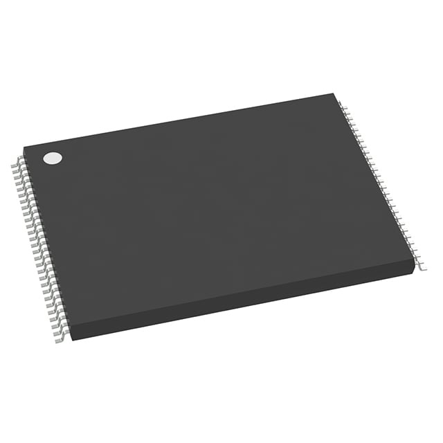
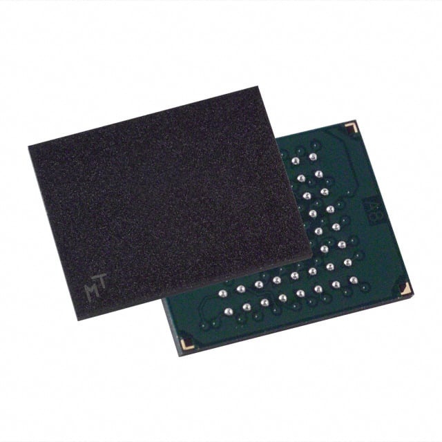
MT28F128J3FS-12 MET
| Part Description |
IC FLASH 128MBIT PARALLEL 64FBGA |
|---|---|
| Quantity | 313 Available (as of June 14, 2026) |

| Product Category | Memory |
|---|---|
| Manufacturer | Micron Technology Inc. |
| Manufacturing Status | Obsolete |
| Manufacturer Standard Lead Time | Contact Us |
| Datasheet |
Specifications & Environmental
| Device Package | 64-FBGA (10x13) | Memory Format | FLASH | Technology | FLASH | ||
|---|---|---|---|---|---|---|---|
| Memory Size | 128 Mbit | Access Time | 120 ns | Grade | Industrial | ||
| Clock Frequency | N/A | Voltage | 2.7V ~ 3.6V | Memory Type | Non-Volatile | ||
| Operating Temperature | -40°C ~ 85°C (TA) | Write Cycle Time Word Page | N/A | Packaging | 64-FBGA | ||
| Mounting Method | Non-Volatile | Memory Interface | Parallel | Memory Organization | 16M x 8, 8M x 16 | ||
| Moisture Sensitivity Level | 2 (1 Year) | RoHS Compliance | RoHS non-compliant | REACH Compliance | REACH Unaffected | ||
| Qualification | N/A | ECCN | 3A991B1A | HTS Code | 8542.32.0071 |
Overview of MT28F128J3FS-12 MET – IC FLASH 128MBIT PARALLEL 64FBGA
The MT28F128J3FS-12 MET is a 128 Mbit, parallel-interface Q-FLASH® memory device in a 64-ball FBGA package. It provides non-volatile FLASH storage with asynchronous page mode read support and a 16M × 8 or 8M × 16 memory organization.
Designed for systems that require parallel NOR-style flash storage, the device combines sector-based erase architecture, on-chip protection features and a wide 2.7 V to 3.6 V operating range to support reliable code and data storage across a wide temperature span.
Key Features
- Memory Architecture — 128 Mbit FLASH organized as 16M × 8 or 8M × 16 with one hundred twenty-eight 128 KB erase blocks for the 128 Mb density.
- Read Performance — Asynchronous page mode reads at 120 ns / 25 ns read access time for the 128 Mb device, supporting fast code fetch and data access patterns.
- Program and Erase — Automatic write and erase algorithms with 5.6 μs-per-byte effective programming time using the write buffer and up to 100,000 erase cycles per block.
- Protection and Identification — 128-bit protection register, 64-bit unique device identifier, and 64-bit user-programmable OTP cells for device authentication and secure storage.
- Enhanced Data Protection — Flexible sector locking, sector erase/program lockout during power transition, and enhanced protection feature when VPEN = VSS.
- Interface and Compatibility — Parallel memory interface with industry-standard pinout; inputs and outputs are fully TTL-compatible. Supports Common Flash Interface (CFI) and Scalable Command Set.
- Voltage and Temperature — VCC, VCCQ, and VPEN operation/programming from 2.7 V to 3.6 V; extended operating temperature range of −40 °C to +85 °C (TA).
- Package — 64-FBGA (10 × 13) ball grid array for compact board-level footprint.
Typical Applications
- Embedded Systems — Parallel FLASH storage for embedded controllers and systems that require non-volatile program or data retention within −40 °C to +85 °C operating range.
- Firmware and Code Storage — Storage of system firmware and boot code with fast asynchronous page-mode reads and sector-based erase granularity.
- Industrial Equipment — Non-volatile storage in industrial environments where extended temperature operation and high erase cycle endurance (100,000 cycles per block) are required.
Unique Advantages
- Flexible Density and Organization — 16M × 8 and 8M × 16 organizations provide designers options for byte- or word-oriented data buses without changing core device family.
- Fast Read Path — 120 ns asynchronous access with a 25 ns page-mode option for the 128 Mb device, enabling faster code fetches in parallel-memory systems.
- Robust Endurance — Up to 100,000 erase cycles per block and automatic erase/program algorithms to support long service life for frequently updated sectors.
- On-Chip Security and ID — 128-bit protection register plus 64-bit unique device ID and 64-bit OTP for device identification and secure, non-volatile data storage.
- Broad Voltage Range — 2.7 V to 3.6 V operation for compatibility with common 3 V system domains and programming operations.
- Compact FBGA Package — 64-ball FBGA (10 × 13) package provides a small board footprint while maintaining industry-standard pinout for parallel flash deployment.
Why Choose IC FLASH 128MBIT PARALLEL 64FBGA?
The MT28F128J3FS-12 MET is positioned as a reliable 128 Mbit parallel FLASH device in Micron’s Q-FLASH® family, combining sector-based erase architecture, on-chip protection, and industry-standard parallel interfacing. Its combination of read performance, write-buffer programming efficiency, and extended temperature operation makes it suitable for designs that require robust non-volatile storage and predictable behavior across a range of operating conditions.
This device is appropriate for engineers specifying parallel NOR-style flash for firmware, code shadowing, or data storage in embedded and industrial systems. The array of protection features, unique ID and OTP cells, and high erase endurance support long-term deployment and device traceability within product lifecycles.
Request a quote or submit an inquiry to obtain pricing and availability for the MT28F128J3FS-12 MET and to discuss integration details for your design.