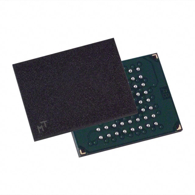
MT28F128J3BS-12 MET
| Part Description |
IC FLASH 128MBIT PARALLEL 64FBGA |
|---|---|
| Quantity | 897 Available (as of June 15, 2026) |

| Product Category | Memory |
|---|---|
| Manufacturer | Micron Technology Inc. |
| Manufacturing Status | Obsolete |
| Manufacturer Standard Lead Time | Contact Us |
| Datasheet |
Specifications & Environmental
| Device Package | 64-FBGA (10x13) | Memory Format | FLASH | Technology | FLASH | ||
|---|---|---|---|---|---|---|---|
| Memory Size | 128 Mbit | Access Time | 120 ns | Grade | Industrial | ||
| Clock Frequency | N/A | Voltage | 2.7V ~ 3.6V | Memory Type | Non-Volatile | ||
| Operating Temperature | -40°C ~ 85°C (TA) | Write Cycle Time Word Page | N/A | Packaging | 64-FBGA | ||
| Mounting Method | Non-Volatile | Memory Interface | Parallel | Memory Organization | 16M x 8, 8M x 16 | ||
| Moisture Sensitivity Level | 4 (72 Hours) | RoHS Compliance | ROHS3 Compliant | REACH Compliance | REACH Unaffected | ||
| Qualification | N/A | ECCN | 3A991B1A | HTS Code | 8542.32.0071 |
Overview of MT28F128J3BS-12 MET – IC FLASH 128MBIT PARALLEL 64FBGA
The MT28F128J3BS-12 MET is a 128 Mbit non-volatile FLASH memory device in a 64-ball FBGA package. It is organized as 16M × 8 or 8M × 16 and implements a parallel memory interface with asynchronous page-mode reads.
Designed for systems that require parallel FLASH storage, the device offers a 2.7 V to 3.6 V supply range, -40°C to +85°C operating tolerance, and a 120 ns read access time (128 Mb option), providing a balance of performance, endurance, and on-board protection features.
Key Features
- Memory Type & Capacity 128 Mbit FLASH non-volatile memory with memory organization options of 16M × 8 or 8M × 16 and one hundred twenty-eight 128 KB erase blocks for the 128 Mb device.
- Interface & Read Performance Parallel memory interface supporting asynchronous page-mode reads; 120 ns/25 ns read access time specified for the 128 Mb device.
- Program/Erase Efficiency Automatic write and erase algorithm with a 5.6 μs-per-byte effective programming time when using the write buffer.
- Protection & Identification 128-bit protection register, 64-bit unique device identifier and 64-bit user-programmable OTP cells for secure device ID and configuration storage.
- Power VCC and programming operation supported from 2.7 V to 3.6 V.
- Endurance & Suspend Options 100,000 erase cycles per block and automatic suspend capabilities including block erase suspend-to-read, block erase suspend-to-program, and program suspend-to-read.
- Data Integrity Features Enhanced data protection with VPEN = VSS, flexible sector locking, and sector erase/program lockout during power transition.
- Package & I/O 64-ball FBGA (10 × 13) package; inputs and outputs are fully TTL-compatible and the device uses an industry-standard pinout.
- Command & Identification Common Flash Interface (CFI) and Scalable Command Set support; manufacturer ID codes include Micron (0x2C) and Intel (0x89).
Typical Applications
- Embedded systems Parallel FLASH storage for systems operating within -40°C to +85°C and 2.7 V–3.6 V supply ranges.
- In-system code storage Parallel interface and 120 ns access time support execution and lookup use cases where asynchronous reads are required.
- Device identification & configuration On-chip 64-bit unique identifier and 64-bit OTP cells for secure ID, traceability, or one-time programmable settings.
- Field updatable firmware Write-buffer programming and block erase/program suspend options facilitate in-field updates while allowing read access during erase/program operations.
Unique Advantages
- Flexible memory organization: 16M × 8 or 8M × 16 options allow matching the device data width to system bus requirements.
- Low-latency parallel reads: 120 ns access time (128 Mb) for faster asynchronous page-mode read performance.
- On-chip protection features: 128-bit protection register, sector locking, and enhanced VPEN protection reduce risk of accidental writes or erases.
- High block endurance: 100,000 erase cycles per block supports frequent update scenarios.
- Compact package footprint: 64-ball FBGA (10 × 13) offers a small-board implementation with TTL-compatible I/O.
- Standardized integration: CFI and Scalable Command Set support simplifies device identification and command-level integration into existing designs.
Why Choose IC FLASH 128MBIT PARALLEL 64FBGA?
The MT28F128J3BS-12 MET positions itself as a robust parallel FLASH memory option combining 128 Mbit capacity, flexible data-width organization, and a compact 64-ball FBGA footprint. Its 2.7 V–3.6 V operation range, -40°C to +85°C rating, and integrated protection features make it suitable for designs that require reliable non-volatile storage with controlled access and endurance.
This device is appropriate for engineers and procurement teams specifying parallel FLASH for systems needing standardized command support (CFI/Scalable Command Set), device identification, and in-system update capability while maintaining TTL-compatible I/O and a small PCB footprint.
Request a quote or submit an inquiry for availability and volume pricing for the MT28F128J3BS-12 MET to evaluate suitability for your design and procurement needs.