
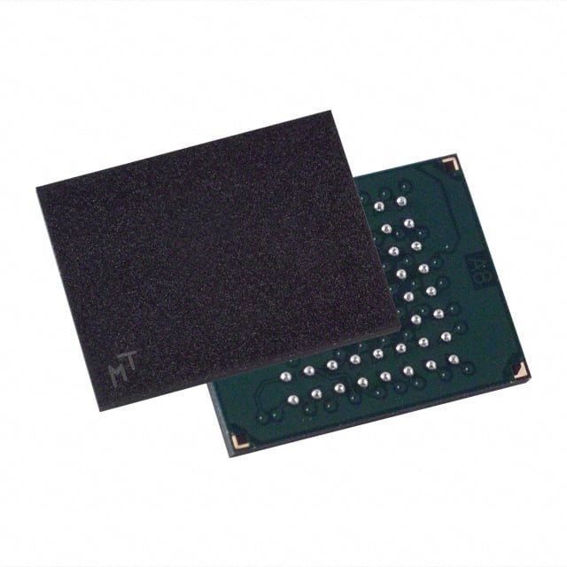
M56Z8G32256A (2H)
| Part Description |
LPDDR4x SDRAM |
|---|---|
| Quantity | 529 Available (as of June 15, 2026) |

| Product Category | Memory |
|---|---|
| Manufacturer | ESMT |
| Manufacturing Status | Active |
| Manufacturer Standard Lead Time | Contact Us |
| Datasheet |
Specifications & Environmental
| Device Package | 200 Ball BGA | Memory Format | DRAM | Technology | DRAM - LPDDR4X | ||
|---|---|---|---|---|---|---|---|
| Memory Size | 8 Gbit | Access Time | 3.5 ns | Grade | Commercial | ||
| Clock Frequency | 2.133 GHz | Voltage | 1.70V ~ 1.95V | Memory Type | Volatile | ||
| Operating Temperature | -25°C – 85°C | Write Cycle Time Word Page | 18 ns | Packaging | 200 Ball BGA | ||
| Mounting Method | Surface Mount | Memory Interface | LPDDR4X | Memory Organization | 256M x 32 | ||
| Moisture Sensitivity Level | 3 | RoHS Compliance | Compliant | REACH Compliance | REACH Unknown | ||
| Qualification | JEDEC | ECCN | EAR99 | HTS Code | 8542.32.00.36 |
Overview of M56Z8G32256A (2H) – LPDDR4x SDRAM
The M56Z8G32256A (2H) is an LPDDR4x SDRAM device providing 8.59 Gbit of volatile DRAM in a 256M × 32 organization (256M16 × 2 die in package, two channels × 16 I/O). Built on LPDDR4/LPDDR4X architecture, the device supports high data-rate operation with low-voltage core and I/O supplies for systems that require compact, low-power, high-bandwidth memory.
Clocked at 2.133 GHz (2133 MHz) with a data rate of 4266 Mbps per pin and an access time of 3.5 ns, this device targets designs that need programmable latencies, concurrent bank operation, and advanced power-management features within a commercial temperature range.
Key Features
- Core and Architecture 16n prefetch DDR architecture with 8 internal banks per channel to support concurrent bank operation and efficient command scheduling.
- Memory Organization 256M × 32 organization (256M16 × 2 die in package) delivering 8.59 Gbit total capacity and dual-channel (2 channels × 16 I/O) device configuration.
- Performance 2.133 GHz clock frequency (2133 MHz) with 4266 Mbps per pin data rate and up to 8.5 GB/s per die; programmable READ/WRITE latencies and on-the-fly burst lengths (BL = 16, 32).
- Power Ultra-low-voltage core and I/O supply ranges: VDD1 = 1.70–1.95 V (nominal 1.80 V); VDD2 = 1.06–1.17 V (nominal 1.10 V); VDDQ = 1.06–1.17 V (nominal 1.10 V) or low VDDQ = 0.57–0.65 V (nominal 0.60 V).
- Reliability & Memory Management Directed per-bank refresh and partial-array self refresh (PASR) for flexible refresh management plus an on-chip temperature sensor to control self-refresh rate.
- Interfaces & I/O LPDDR4X interface with bidirectional/differential data strobe per byte lane, selectable output drive strength (DS), and programmable VSS (ODT) termination.
- Packaging & Mounting 200 Ball BGA package, surface-mount mounting type, JEDEC qualification and RoHS-compliant packaging.
- Operating Range Commercial grade operating temperature range of −25 °C to +85 °C.
Typical Applications
- High-Bandwidth Memory Subsystems — Use where sustained high transfer rates are required, leveraging 4266 Mbps per pin and up to 8.5 GB/s per die.
- Low-Power Designs — Systems that need reduced power consumption can take advantage of the LPDDR4x ultra-low-voltage supplies and low VDDQ options.
- Concurrent-Memory Operation — Multi-bank, dual-channel architectures benefit from 8 internal banks per channel and directed per-bank refresh for improved command scheduling.
Unique Advantages
- High data throughput: 2.133 GHz clock and 4266 Mbps per pin data rate deliver significant bandwidth for memory-intensive tasks.
- Flexible latency and bursting: Programmable READ/WRITE latencies and burst lengths (BL = 16, 32) enable designers to tune performance to workload requirements.
- Advanced power management: Multiple VDDQ options, PASR, clock-stop capability and an on-chip temperature sensor help optimize power consumption and refresh behavior.
- Robust memory organization: 256M × 32 memory organization with dual ×16 die configuration supports scalable capacity and channeling for system designs.
- Industry-standard compliance: JEDEC qualification and RoHS-compliant packaging provide predictable integration and regulatory conformity for commercial designs.
Why Choose M56Z8G32256A (2H)?
The M56Z8G32256A (2H) positions itself as a high-bandwidth, low-voltage LPDDR4x SDRAM option for commercial designs that require programmable performance, robust refresh control, and flexible power modes. Its dual-die, dual-channel organization and on-chip management features make it suitable for systems that need concurrent memory operations and tunable latency.
With JEDEC qualification, RoHS compliance, and a 200 Ball BGA surface-mount package, the device supports straightforward integration into compact PCBs while offering specifications that help balance throughput, power efficiency, and thermal-aware refresh control across the −25 °C to +85 °C operating range.
Request a quote or submit an inquiry to obtain pricing, availability, and ordering information for the M56Z8G32256A (2H) LPDDR4x SDRAM.


Date Founded: 1998
Headquarters: Hsinchu Science Park, Hsinchu, Taiwan
Employees: 400+
Revenue: $377.8 Million
Certifications and Memberships: N/A


