
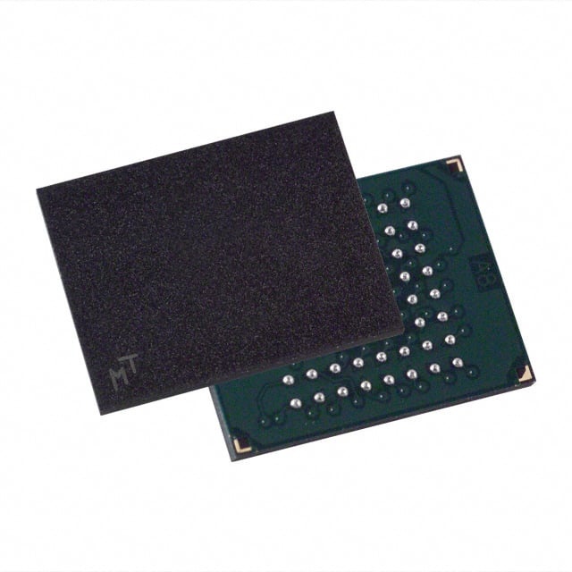
M56Z8G32256A
| Part Description |
LPDDR4x SDRAM |
|---|---|
| Quantity | 575 Available (as of June 9, 2026) |

| Product Category | Memory |
|---|---|
| Manufacturer | ESMT |
| Manufacturing Status | Active |
| Manufacturer Standard Lead Time | Contact Us |
| Datasheet |
Specifications & Environmental
| Device Package | 200 Ball BGA | Memory Format | DRAM | Technology | DRAM - LPDDR4X | ||
|---|---|---|---|---|---|---|---|
| Memory Size | 8 Gbit | Access Time | 3.5 ns | Grade | Commercial | ||
| Clock Frequency | 1.866 GHz | Voltage | 1.70V ~ 1.95V | Memory Type | Volatile | ||
| Operating Temperature | -25°C – 85°C | Write Cycle Time Word Page | 18 ns | Packaging | 200 Ball BGA | ||
| Mounting Method | Surface Mount | Memory Interface | LPDDR4X | Memory Organization | 256M x 32 | ||
| Moisture Sensitivity Level | 3 | RoHS Compliance | Compliant | REACH Compliance | REACH Unknown | ||
| Qualification | JEDEC | ECCN | EAR99 | HTS Code | 8542.32.00.36 |
Overview of M56Z8G32256A – LPDDR4x SDRAM
The M56Z8G32256A is an 8.59 Gbit LPDDR4/LPDDR4X SDRAM device organized as 256M × 32 (2 channels × 16 I/O). It combines high data throughput with ultra-low-voltage operation to serve designs that require high-bandwidth volatile memory in a compact package.
Built with a 16n prefetch DDR architecture and dual ×16 die configuration in-package, this JEDEC-qualified commercial-grade memory delivers programmable latencies, per-bank refresh control, and on-chip temperature monitoring for controlled self-refresh behavior.
Key Features
- Core & Memory Architecture 256M × 32 organization (256M16 × 2 die in package), 16n prefetch DDR architecture and 8 internal banks per channel for concurrent bank operation.
- Performance Clock frequency 1.866 GHz (1866 MHz) with a data rate listed at 3733 Mbps/pin; datasheet notes up to 8.5 GB/s per die. Typical access time is 3.5 ns and write cycle time (word page) is 18 ns.
- Programmable Timing & Burst Programmable READ/WRITE latencies (RL/WL) and selectable burst lengths (BL = 16, 32). Example speed grade shows WRITE latency options (Set A = 16, Set B = 30) and READ latency examples (DBI Disabled = 32, DBI Enabled = 36).
- Low-Voltage Power Options Ultra-low-voltage core and I/O supply ranges: VDD1 = 1.70–1.95 V (nominal 1.80 V); VDD2 = 1.06–1.17 V (nominal 1.10 V); VDDQ = 1.06–1.17 V or low VDDQ = 0.57–0.65 V (nominal values noted in datasheet).
- Power Management & Reliability Directed per-bank refresh for concurrent operation, partial-array self-refresh (PASR), on-chip temperature sensor to control self-refresh rate, programmable ODT (VSS), and selectable output drive strength.
- Interface & Signals LPDDR4X interface with bidirectional/differential data strobe per byte lane and single-data-rate CMD/ADR entry; clock-stop capability is supported.
- Package & Environmental 200 Ball BGA surface-mount package, JEDEC-qualified commercial grade, RoHS-compliant. Operating temperature range: −25°C to +85°C.
Unique Advantages
- High sustained bandwidth: The 1866 MHz clock rate and up to 3733 Mbps/pin data rate yield high per-die throughput (up to 8.5 GB/s), enabling demanding memory bandwidth needs.
- Flexible latency and burst control: Programmable RL/WL and multiple burst-length options allow tuning of timing for system-level performance and power trade-offs.
- Power-scalable operation: Multiple supply voltage ranges (including low VDDQ option) and clock-stop capability help reduce system power across operating modes.
- Granular refresh control: Directed per-bank refresh and PASR support reduce refresh impact on active banks, improving effective memory availability.
- Thermal-aware behavior: On-chip temperature sensor adjusts self-refresh behavior to maintain data retention and energy efficiency over temperature variations.
- Compact surface-mount package: 200 Ball BGA package provides a high-density footprint suitable for space-constrained system designs.
Why Choose M56Z8G32256A?
The M56Z8G32256A positions itself as a high-performance, low-voltage LPDDR4/LPDDR4X SDRAM solution for designs that require significant bandwidth, configurable timing, and power-optimized operation. Its dual-die, 256M × 32 organization and programmable features make it suitable for systems that need concurrent bank operation, flexible latency tuning, and robust refresh management.
Backed by JEDEC qualification and RoHS-compliant packaging, the M56Z8G32256A is suited to commercial-grade products where predictable timing options, thermal-aware self-refresh, and a compact 200 Ball BGA footprint are important for long-term deployment and supply-chain integration.
Request a quote or submit an inquiry for pricing, availability, and additional technical details regarding the M56Z8G32256A LPDDR4x SDRAM.


Date Founded: 1998
Headquarters: Hsinchu Science Park, Hsinchu, Taiwan
Employees: 400+
Revenue: $377.8 Million
Certifications and Memberships: N/A


