
M56Z4G16256A2H
| Part Description |
LPDDR4x SDRAM |
|---|---|
| Quantity | 741 Available (as of June 8, 2026) |

| Product Category | Memory |
|---|---|
| Manufacturer | ESMT |
| Manufacturing Status | Active |
| Manufacturer Standard Lead Time | Contact Us |
| Datasheet |
Specifications & Environmental
| Device Package | 200 Ball BGA | Memory Format | DRAM | Technology | DRAM - LPDDR4X | ||
|---|---|---|---|---|---|---|---|
| Memory Size | 4 Gbit | Access Time | 3.5 ns | Grade | Commercial | ||
| Clock Frequency | 2.133 GHz | Voltage | 1.70V ~ 1.95V | Memory Type | Volatile | ||
| Operating Temperature | -25°C – 85°C | Write Cycle Time Word Page | 18 ns | Packaging | 200 Ball BGA | ||
| Mounting Method | Surface Mount | Memory Interface | LPDDR4X | Memory Organization | 256M x 16 | ||
| Moisture Sensitivity Level | 3 | RoHS Compliance | Compliant | REACH Compliance | REACH Unknown | ||
| Qualification | JEDEC | ECCN | EAR99 | HTS Code | 8542.32.00.36 |
Overview of M56Z4G16256A(2H) – LPDDR4x SDRAM
The M56Z4G16256A(2H) is an LPDDR4x SDRAM device from ESMT offering a 4.295 Gbit memory capacity in a 256M × 16 organization. It combines LPDDR4x architecture with a 16n prefetch DDR core and multiple power domains for high-bandwidth, low-voltage operation.
Designed for systems that require high data throughput and power efficiency, the device delivers up to 8.5 GB/s per die, programmable latencies and burst lengths, and JEDEC qualification for straightforward integration into LPDDR4x memory subsystems.
Key Features
- Core & Architecture 16n prefetch DDR architecture with 8 internal banks per channel and single-data-rate CMD/ADR entry to support concurrent bank operation and efficient command scheduling.
- Memory Organization & Capacity 4.295 Gbit total capacity implemented as 256M × 16 (one channel × 16 I/O); device configured as 256M16 × 1 die in package.
- Performance Clock frequency specified at 2.133 GHz with rated data rate up to 4266 Mbps/pin (ordering information); up to 8.5 GB/s per die throughput.
- Timing Access time 3.5 ns, write cycle time (word/page) 18 ns, and programmable READ/WRITE latencies (RL/WL). Speed grade cycle times include 535 ps @ RL = 32/36 and 468 ps @ RL = 36/40.
- Power Domains & Voltage Ultra-low-voltage operation with VDD1 = 1.70–1.95 V (1.80 V nominal), VDD2 = 1.06–1.17 V (1.10 V nominal), and VDDQ options including 1.06–1.17 V or low VDDQ = 0.57–0.65 V.
- Data Interface LPDDR4X interface with bidirectional/differential data strobe per byte lane and programmable burst lengths (BL = 16, 32) for flexible data transfers.
- Refresh & Power Management Directed per-bank refresh for concurrent bank operation, partial-array self refresh (PASR), on-chip temperature sensor to control self-refresh rate, and clock-stop capability for power savings.
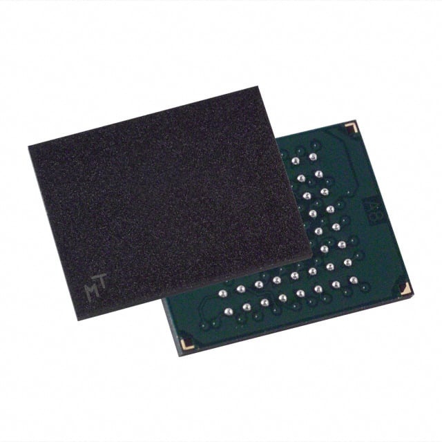
- Packaging & Mounting 200 Ball BGA surface-mount package for compact board integration; device configuration and ball descriptions provided for routing and layout.
- Operating Range & Compliance Commercial grade with operating temperature −25 °C to +85 °C and JEDEC qualification; RoHS-compliant packaging.
Typical Applications
- High-bandwidth memory subsystems Use where sustained data throughput is required; the device supports up to 8.5 GB/s per die and programmable burst lengths for optimized transfers.
- Power-sensitive designs Suitable for systems constrained by power budget thanks to LPDDR4x low-voltage domains (VDD1, VDD2, VDDQ) and clock-stop capability to reduce idle power.
- Compact board layouts 200 Ball BGA package enables dense, surface-mount integration on space-constrained PCBs.
- Memory subsystems requiring JEDEC qualification JEDEC-qualified LPDDR4/LPDDR4X device for designs that reference industry-standard specifications.
Unique Advantages
- Low-voltage operation: Reduces system power draw with VDD1 = 1.70–1.95 V and selectable VDDQ options for finer power tuning.
- High data throughput: Up to 8.5 GB/s per die and 2.133 GHz clocking deliver the bandwidth needed for demanding memory transfers.
- Flexible timing and bursts: Programmable RL/WL and selectable burst lengths (BL = 16, 32) let designers tune latency and transfer size for application needs.
- Advanced refresh and power features: Directed per-bank refresh, PASR, and on-chip temperature sensor enable efficient, reliable operation and lower refresh overhead.
- Compact, standardized package: 200 Ball BGA surface-mount package simplifies high-density board designs while maintaining JEDEC compatibility.
- Standards and environmental compliance: JEDEC qualification and RoHS-compliant packaging support regulatory and industry requirements.
Why Choose M56Z4G16256A(2H)?
The M56Z4G16256A(2H) balances high-bandwidth performance with low-voltage operation and flexible timing controls, making it a practical choice for memory subsystems that need measurable throughput and power efficiency. Its LPDDR4x architecture, programmable latencies, and directed per-bank refresh support robust memory scheduling and optimization.
This JEDEC-qualified, RoHS-compliant device in a 200 Ball BGA package is suited to designs that demand compact, surface-mount integration and predictable thermal/voltage behavior across a commercial temperature range. Engineers seeking a scalable LPDDR4x die with on-chip power and refresh features will find the M56Z4G16256A(2H) a technically transparent option for system-level memory design.
Request a quote or submit a product inquiry for M56Z4G16256A(2H) to receive pricing, availability, and ordering details.


Date Founded: 1998
Headquarters: Hsinchu Science Park, Hsinchu, Taiwan
Employees: 400+
Revenue: $377.8 Million
Certifications and Memberships: N/A


