MT29F256G08CKCDBJ5-6R:D TR
| Part Description |
IC FLASH 256GBIT PAR 132TBGA |
|---|---|
| Quantity | 1,261 Available (as of June 15, 2026) |
| Product Category | Flash Memory |
|---|---|
| Manufacturer | Micron Technology Inc. |
| Manufacturing Status | Obsolete |
| Manufacturer Standard Lead Time | Contact Us |
| Datasheet |
Specifications & Environmental
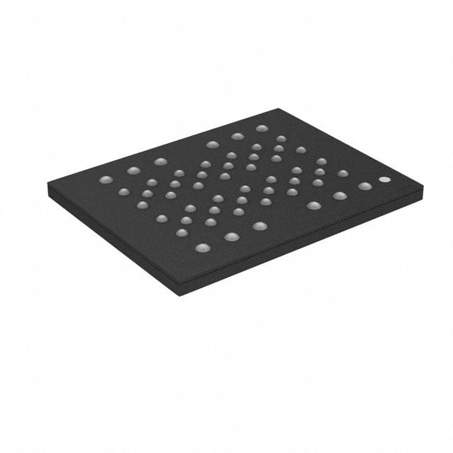
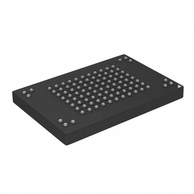
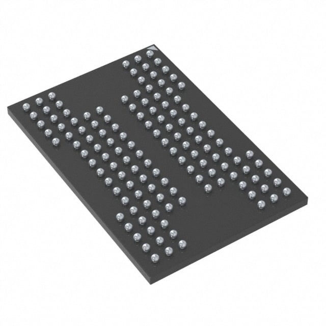
| Device Package | 132-TBGA (12x18) | Memory Format | FLASH | Technology | FLASH - NAND (MLC) | ||
|---|---|---|---|---|---|---|---|
| Memory Size | 256 Gbit | Access Time | N/A | Grade | Commercial | ||
| Clock Frequency | 167 MHz | Voltage | 2.7V ~ 3.6V | Memory Type | Non-Volatile | ||
| Operating Temperature | 0°C ~ 70°C (TA) | Write Cycle Time Word Page | N/A | Packaging | N/A | ||
| Mounting Method | Non-Volatile | Memory Interface | Parallel | Memory Organization | 32G x 8 | ||
| Moisture Sensitivity Level | 3 (168 Hours) | RoHS Compliance | ROHS3 Compliant | REACH Compliance | REACH Unknown | ||
| Qualification | N/A | ECCN | 3A991B1A | HTS Code | 8542.32.0071 |
Overview of MT29F256G08CKCDBJ5-6R:D TR – IC FLASH 256GBIT PAR 132TBGA
The MT29F256G08CKCDBJ5-6R:D TR is a 256 Gbit non-volatile FLASH memory device based on NAND (MLC) technology with a parallel memory interface. It is organized as 32G × 8 and operates with a supply voltage range of 2.7 V to 3.6 V and a clock frequency of 167 MHz.
This device is suited for designs that require high-density parallel NAND storage in a 132-TBGA (12x18) package and operate within a 0°C to 70°C ambient temperature range.
Key Features
- Memory Core 256 Gbit capacity of non-volatile FLASH memory using NAND (MLC) technology, organized as 32G × 8.
- Interface and Performance Parallel memory interface with a specified clock frequency of 167 MHz for synchronous operation.
- Power Operates from a 2.7 V to 3.6 V supply range, compatible with common 3.3 V system voltages.
- Package Supplied in a 132-TBGA package (12x18), providing a defined form factor for board-level integration.
- Operating Temperature Rated for ambient operation from 0°C to 70°C (TA), suitable for standard commercial temperature environments.
- Memory Format FLASH memory format with a parallel interface and multi-level cell (MLC) technology.
Typical Applications
- High-density storage systems Use where 256 Gbit of parallel NAND flash is required for bulk non-volatile storage.
- Embedded devices Integration into embedded platforms that accept a parallel memory interface and operate within 0°C to 70°C.
- Board-level flash integration Suitable for designs calling for a 132-TBGA (12x18) package footprint and a 2.7 V–3.6 V power domain.
Unique Advantages
- High storage density: 256 Gbit capacity reduces the need for multiple devices to achieve large non-volatile storage pools.
- Parallel interface support: Parallel memory organization and a 167 MHz clock enable integration with systems that use parallel NAND connectivity.
- Flexible power range: 2.7 V–3.6 V supply range allows compatibility with common 3.3 V system rails.
- Defined package footprint: 132-TBGA (12x18) package simplifies mechanical planning and PCB layout for board-level assembly.
- Commercial temperature rating: 0°C–70°C ambient rating aligns with standard commercial operating environments.
Why Choose MT29F256G08CKCDBJ5-6R:D TR?
The MT29F256G08CKCDBJ5-6R:D TR provides a high-density, parallel-interface NAND solution in a 132-TBGA footprint, delivering 256 Gbit of MLC FLASH storage with a 167 MHz clock and a 2.7 V–3.6 V supply range. Its 32G × 8 organization and commercial temperature rating make it a straightforward option for designs that require large-capacity non-volatile memory within defined power and temperature envelopes.
This device is well suited to engineering teams and procurement seeking a documented high-capacity parallel NAND FLASH device for board-level integration where the listed electrical, thermal, and packaging specifications match system requirements.
Request a quote or contact sales to obtain pricing, availability, and additional procurement information for the MT29F256G08CKCDBJ5-6R:D TR.