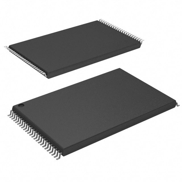
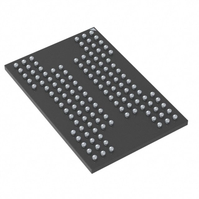
MT29F32G08ABAAAM73A3WC1
| Part Description |
IC FLASH 32GBIT PARALLEL DIE |
|---|---|
| Quantity | 790 Available (as of June 15, 2026) |

| Product Category | Flash Memory |
|---|---|
| Manufacturer | Micron Technology Inc. |
| Manufacturing Status | Obsolete |
| Manufacturer Standard Lead Time | Contact Us |
| Datasheet |
Specifications & Environmental
| Device Package | Die | Memory Format | FLASH | Technology | FLASH - NAND | ||
|---|---|---|---|---|---|---|---|
| Memory Size | 32 Gbit | Access Time | N/A | Grade | Commercial | ||
| Clock Frequency | N/A | Voltage | 2.7V ~ 3.6V | Memory Type | Non-Volatile | ||
| Operating Temperature | 0°C ~ 70°C (TA) | Write Cycle Time Word Page | N/A | Packaging | Die | ||
| Mounting Method | Non-Volatile | Memory Interface | Parallel | Memory Organization | 4G x 8 | ||
| Moisture Sensitivity Level | 3 (168 Hours) | RoHS Compliance | ROHS3 Compliant | REACH Compliance | REACH Unknown | ||
| Qualification | N/A | ECCN | 3A991B1A | HTS Code | 8542.32.0071 |
Overview of MT29F32G08ABAAAM73A3WC1 – IC FLASH 32GBIT PARALLEL DIE
The MT29F32G08ABAAAM73A3WC1 is a 32 Gbit non-volatile NAND flash die from Micron Technology. It implements single-level cell (SLC) NAND architecture in a 4G × 8 organization with a parallel interface, delivering a compact die form factor for integration into embedded storage designs that require on‑chip non-volatile memory.
Designed for systems operating at standard commercial temperatures, the device combines ONFI-compliant command support and advanced NAND commands to address firmware, data storage and system flash requirements where endurance, interface flexibility and integration density matter.
Key Features
- Memory Core — 32 Gbit capacity organized as 4G × 8 with single-level cell (SLC) NAND technology for non-volatile data storage.
- ONFI 2.2 Compliance & Command Set — Supports the ONFI NAND Flash Protocol and an advanced command set including program cache, read cache (sequential and random), one-time programmable (OTP) mode, multi-plane and multi-LUN operations, read unique ID and copyback.
- Page / Block / Plane Organization — Page size (×8): 8,640 bytes (8,192 + 448), block size: 128 pages (1,024K + 56K bytes), and 2 planes × 2,048 blocks per plane (device = 4,096 blocks for 32Gb).
- Synchronous and Asynchronous I/O — Synchronous operation up to timing mode 5 with DDR-capable 10 ns clock (read/write throughput per pin up to 200 MT/s); asynchronous I/O up to timing mode 5 with per-pin throughput up to 50 MT/s.
- Array Performance — Typical array timings include read page: 35 μs (max specified), program page: ~350 μs (typical), and erase block: ~1.5 ms (typical).
- Endurance & Data Retention — Rated endurance of 80,000 program/erase cycles with data retention and qualification information referenced in the datasheet.
- Power and I/O Voltage — VCC operating range 2.7 V to 3.6 V; VCCQ supported at 1.7–1.95 V and 2.7–3.6 V (per device configuration).
- Package & Temperature — Supplied as a die for direct integration; specified commercial operating temperature 0 °C to +70 °C (TA).
Typical Applications
- Embedded Storage — Firmware and persistent data storage in embedded systems that require a parallel NAND die for on‑board integration.
- Consumer Electronics — On‑die non‑volatile memory for consumer devices operating within the specified commercial temperature range.
- Memory Module Integration — Integration into custom memory modules or multi‑die solutions where a 32 Gbit parallel NAND die is required.
Unique Advantages
- ONFI 2.2 interoperability: Ensures compatibility with ONFI‑compliant controllers and tooling for standardized command and timing support.
- SLC NAND endurance: 80,000 program/erase cycles provide longevity for applications with frequent updates to flash content.
- Dual I/O modes: Both synchronous (DDR) and asynchronous interfaces allow designers to choose between higher throughput (up to 200 MT/s per pin) and legacy asynchronous operation (up to 50 MT/s per pin).
- Advanced NAND commands: Features such as program/read cache, multi‑plane and multi‑LUN operations, OTP and copyback reduce host overhead and enable efficient memory management.
- Compact die form: Supplied as a die for direct integration into custom assemblies or multi‑die packages, simplifying BOM when die‑level integration is required.
Why Choose MT29F32G08ABAAAM73A3WC1?
The MT29F32G08ABAAAM73A3WC1 positions itself as a purpose-built 32 Gbit SLC NAND die offering ONFI‑compliant interfaces, flexible synchronous/asynchronous I/O modes and a command set focused on efficient flash management. Its endurance rating and detailed array performance figures make it suitable for designs that require predictable program/erase behavior and control over memory operations.
This die is intended for designers and integrators who need a compact, high‑endurance NAND building block with standardized protocol support and advanced NAND features. With specified voltage ranges and commercial temperature operation, it supports integration into a wide range of board‑level storage solutions.
Request a quote or submit an inquiry to receive pricing and availability information for MT29F32G08ABAAAM73A3WC1.