MT29F32G08ABAAAWP-IT:A TR
| Part Description |
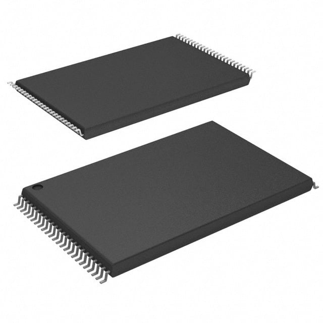
IC FLASH 32GBIT PAR 48TSOP I |
|---|---|
| Quantity | 103 Available (as of June 17, 2026) |

| Product Category | Flash Memory |
|---|---|
| Manufacturer | Micron Technology Inc. |
| Manufacturing Status | Obsolete |
| Manufacturer Standard Lead Time | Contact Us |
| Datasheet |
Specifications & Environmental
| Device Package | 48-TSOP I | Memory Format | FLASH | Technology | FLASH - NAND | ||
|---|---|---|---|---|---|---|---|
| Memory Size | 32 Gbit | Access Time | N/A | Grade | Industrial | ||
| Clock Frequency | N/A | Voltage | 2.7V ~ 3.6V | Memory Type | Non-Volatile | ||
| Operating Temperature | -40°C ~ 85°C (TA) | Write Cycle Time Word Page | N/A | Packaging | 48-TFSOP (0.724", 18.40mm Width) | ||
| Mounting Method | Non-Volatile | Memory Interface | Parallel | Memory Organization | 4G x 8 | ||
| Moisture Sensitivity Level | 3 (168 Hours) | RoHS Compliance | ROHS3 Compliant | REACH Compliance | REACH Unknown | ||
| Qualification | N/A | ECCN | 3A991B1A | HTS Code | 8542.32.0071 |
Overview of MT29F32G08ABAAAWP-IT:A TR – 32Gbit Parallel NAND Flash, 48‑TSOP I
The MT29F32G08ABAAAWP-IT:A TR is a 32 Gbit non-volatile NAND Flash memory in a 48‑TSOP I package. It implements single-level cell (SLC) NAND architecture with a parallel interface and 4G × 8 memory organization for high-density embedded storage.
Designed for industrial-temperature operation (−40°C to +85°C) and a 2.7 V–3.6 V supply range, this device targets embedded and industrial storage applications that require reliable, high-endurance flash in a compact package.
Key Features
- Core / Architecture Single-level cell (SLC) NAND flash with 4G × 8 organization providing 32 Gbit of non-volatile storage capacity.
- Memory Structure Page size x8: 8,640 bytes (8,192 + 448), block size: 128 pages, plane configuration: 2 planes × 2,048 blocks per plane; device size 32Gb: 4,096 blocks.
- Performance (Asynchronous & Synchronous) Supports asynchronous and synchronous I/O modes. Asynchronous throughput up to 50 MT/s per pin; synchronous operation up to timing mode 5 with read/write throughput up to 200 MT/s per pin and DDR‑capable clock (10 ns).
- Program / Erase / Read Timing Read page: up to 35 μs (max), Program page: ~350 μs (typ), Erase block: ~1.5 ms (typ).
- Command and Advanced Functions Implements ONFI 2.2‑compliant command set and supports advanced operations including program cache, read cache (sequential and random), multi‑plane and multi‑LUN commands, copyback, OTP mode and read unique ID.
- Power Operating voltage VCC: 2.7–3.6 V (VCCQ options referenced in device documentation), suitable for standard 3.3 V systems.
- Reliability & Endurance Rated endurance of 80,000 program/erase cycles and data retention consistent with JEDEC/JESD47G guidance as noted in the product documentation.
- Package & Temperature 48‑TSOP I package (0.724", 18.40 mm width) optimized for space‑constrained board designs; industrial operating temperature range −40°C to +85°C.
Typical Applications
- Industrial Embedded Storage Persistent storage for industrial controllers and embedded systems that require SLC endurance and operation across −40°C to +85°C.
- Firmware and Boot Storage Store boot code, firmware images and lookup tables using the device’s OTP and read‑unique‑ID capabilities and first‑block validity at shipment.
- Data Logging and Edge Storage High‑endurance SLC NAND supports sustained program/erase cycles for logging environments and edge devices with frequent writes.
- Storage Subsystems and Controllers Use in designs that leverage parallel NAND interfaces, ONFI interoperability and multi‑plane/multi‑LUN operations for controller integration.
Unique Advantages
- High density in a compact package: 32 Gbit capacity in a 48‑TSOP I form factor enables significant storage without large PCB footprint.
- SLC endurance: Rated for 80,000 program/erase cycles, supporting demanding write‑intensive use cases.
- ONFI 2.2 compatibility: Standardized interface support promotes interoperability with controllers and host designs that support ONFI.
- Flexible I/O modes: Both asynchronous and synchronous operation (including DDR and timing mode 5) allow designers to balance throughput and system timing requirements.
- Industrial temperature operation: −40°C to +85°C rating supports deployments in harsher environments.
- Advanced flash functions: Program/read caches, multi‑plane operations, copyback and OTP provide system design flexibility and performance optimizations.
Why Choose MT29F32G08ABAAAWP-IT:A TR?
The MT29F32G08ABAAAWP-IT:A TR combines SLC NAND endurance, flexible synchronous/asynchronous interfaces and ONFI 2.2 compatibility in a compact 48‑TSOP I package. Its 32 Gbit capacity and documented timing/latency characteristics make it a practical choice for embedded and industrial designs that need reliable non‑volatile storage with robust program/erase endurance.
This device is suited to engineers building firmware storage, data logging, or storage controller applications where industrial temperature range and standardized interface support are required. Product documentation provides device‑level electrical and timing details to aid integration and long‑term design planning.
Request a quote or submit an inquiry to receive pricing and availability for MT29F32G08ABAAAWP-IT:A TR and to discuss volume, lead time, or technical questions.