MT29F32G08ABEABM73A3WC1
| Part Description |
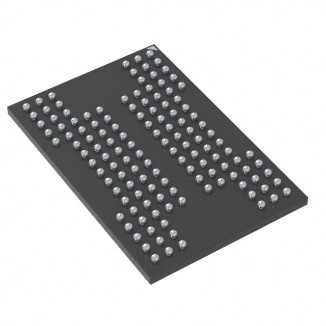
IC FLASH 32GBIT PARALLEL DIE |
|---|---|
| Quantity | 706 Available (as of June 14, 2026) |

| Product Category | Memory |
|---|---|
| Manufacturer | Micron Technology Inc. |
| Manufacturing Status | Obsolete |
| Manufacturer Standard Lead Time | Contact Us |
| Datasheet |
Specifications & Environmental
| Device Package | Die | Memory Format | FLASH | Technology | FLASH - NAND | ||
|---|---|---|---|---|---|---|---|
| Memory Size | 32 Gbit | Access Time | N/A | Grade | Commercial | ||
| Clock Frequency | N/A | Voltage | 2.7V ~ 3.6V | Memory Type | Non-Volatile | ||
| Operating Temperature | 0°C ~ 70°C (TA) | Write Cycle Time Word Page | N/A | Packaging | Die | ||
| Mounting Method | Non-Volatile | Memory Interface | Parallel | Memory Organization | 4G x 8 | ||
| Moisture Sensitivity Level | 3 (168 Hours) | RoHS Compliance | ROHS Compliant | REACH Compliance | REACH Unknown | ||
| Qualification | N/A | ECCN | 3A991B1A | HTS Code | 8542.32.0071 |
Overview of MT29F32G08ABEABM73A3WC1 – IC FLASH 32GBIT PARALLEL DIE
The MT29F32G08ABEABM73A3WC1 is a 32 Gbit non-volatile NAND flash die offered by Micron Technology. It is organized as 4G × 8 and implements asynchronous and synchronous NAND architectures with a parallel memory interface.
Designed for die-level integration, the device provides a high-density NAND option with standard commercial operating conditions and support for advanced NAND command and cache features for embedded storage implementations.
Key Features
- Memory Type & Organization Non-volatile NAND flash organized as 4G × 8 delivering 32 Gbit capacity (32Gb).
- Flash Architecture Single-level cell (SLC) technology with ONFI 2.2-compliant interface and support for both asynchronous and synchronous I/O modes.
- Page / Block / Plane Geometry Page size (x8): 8,640 bytes (8,192 + 448 bytes); block size: 128 pages (1,024K + 56K bytes); device (32Gb) contains 4,096 blocks and 2 planes × 2,048 blocks per plane.
- Synchronous Performance Synchronous timing up to mode 5 with DDR clock rate of 10 ns and read/write throughput per pin up to 200 MT/s; data strobe (DQS) signals support hardware synchronization.
- Asynchronous Performance Asynchronous timing up to mode 5 with read/write throughput per pin up to 50 MT/s and RC/WC minimum of 20 ns.
- Array Performance Read page: up to 35 μs (MAX); program page: ~350 μs (TYP); erase block: ~1.5 ms (TYP).
- Advanced Command Set Program cache, read cache (sequential and random), OTP mode, multi-plane commands, multi-LUN operations, read unique ID, and copyback operations within a plane.
- Reliability & Endurance Endurance rated at 80,000 program/erase cycles and data retention compliant with JESD47G (see qualification report).
- Voltage & Power Operating VCC range: 2.7–3.6 V; VCCQ options include 1.7–1.95 V or 2.7–3.6 V as defined in the device family documentation.
- Operating Temperature Commercial operating temperature range: 0°C to +70°C (TA).
- Package Supplied as a die for direct integration into customer packages and modules.
- Startup & Status RESET (FFh) required as first command after power-on; an operation status byte provides software-based completion, pass/fail, and write-protect status indicators.
Typical Applications
- Embedded Storage High-density non-volatile storage where die-level NAND integration is required for custom module or board-level designs.
- Commercial Electronics Commercial-temperature systems needing parallel NAND flash with synchronous and asynchronous I/O options.
- High-Reliability Embedded Systems Designs that benefit from documented endurance (80,000 P/E cycles) and JESD47G-compliant data retention.
Unique Advantages
- High Density in Die Form 32 Gbit capacity in a die package enables compact, high-density storage integration for custom assemblies.
- Flexible I/O Modes Support for both synchronous (DDR) and asynchronous interfaces lets designers choose between higher throughput or legacy timing compatibility.
- Advanced Data Management On-die features such as program/read cache, OTP, multi-plane and multi-LUN commands simplify data flow and block management.
- Deterministic Array Timing Published read, program, and erase timing (typical and maximum) support predictable performance planning and system-level timing budgets.
- Robust Endurance and Retention Documented 80,000 program/erase cycles and JESD47G data retention compliance support long-term data integrity requirements.
- Standard Voltage Range 2.7–3.6 V supply compatibility aligns with common system power rails for straightforward integration.
Why Choose MT29F32G08ABEABM73A3WC1?
The MT29F32G08ABEABM73A3WC1 provides a compact, die-level 32 Gbit NAND flash solution suited to designs requiring parallel interface NAND with both synchronous and asynchronous operation modes. Its documented endurance, data retention compliance, and detailed timing figures make it appropriate for commercial embedded storage designs where predictability and integration flexibility matter.
This part is aimed at engineers integrating high-density NAND at the die level who need clear electrical, timing, and command-set information to support module or custom package designs within the commercial temperature range.
Request a quote or submit a product inquiry to receive pricing and availability details for MT29F32G08ABEABM73A3WC1.