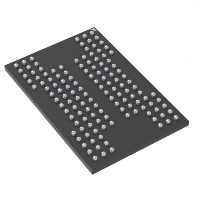
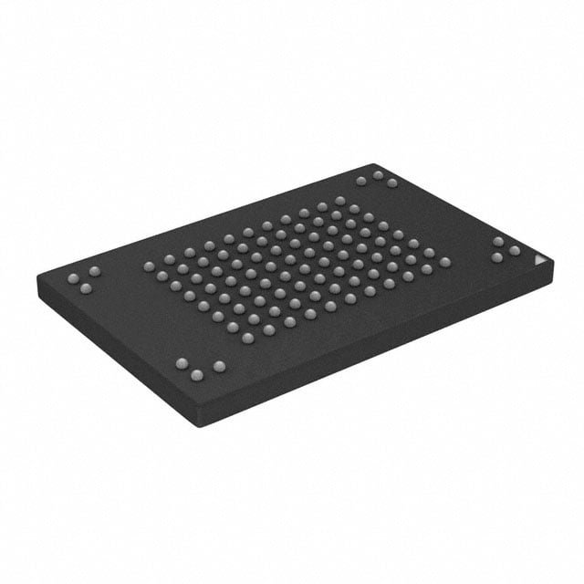
MT29F32G08ABEABM73A3WC1L
| Part Description |
IC FLASH 32GBIT DIE |
|---|---|
| Quantity | 1,127 Available (as of June 14, 2026) |

| Product Category | Memory |
|---|---|
| Manufacturer | Micron Technology Inc. |
| Manufacturing Status | Active |
| Manufacturer Standard Lead Time | 13 Weeks |
| Datasheet |
Specifications & Environmental
| Device Package | Die | Memory Format | FLASH | Technology | FLASH - NAND (SLC) | ||
|---|---|---|---|---|---|---|---|
| Memory Size | 32 Gbit | Access Time | N/A | Grade | Commercial | ||
| Clock Frequency | N/A | Voltage | N/A | Memory Type | Non-Volatile | ||
| Operating Temperature | 0°C ~ 70°C | Write Cycle Time Word Page | N/A | Packaging | Die | ||
| Mounting Method | Non-Volatile | Memory Interface | N/A | Memory Organization | 4G x 8 | ||
| Moisture Sensitivity Level | 3 (168 Hours) | RoHS Compliance | ROHS Compliant | REACH Compliance | REACH Unaffected | ||
| Qualification | N/A | ECCN | N/A | HTS Code | N/A |
Overview of MT29F32G08ABEABM73A3WC1L – IC FLASH 32GBIT DIE
The MT29F32G08ABEABM73A3WC1L is a 32 Gbit non-volatile NAND flash memory delivered as a die and implemented using single-level cell (SLC) NAND technology. The device is organized as 4G × 8 and supports both asynchronous and synchronous I/O modes with ONFI 2.2 compliance.
This die-form NAND flash targets designs requiring SLC reliability and performance in a raw die format. Key value propositions include SLC endurance, multi-mode I/O performance, and an advanced command set for flexible block and plane management.
Key Features
- Memory Type & Capacity 32 Gbit SLC NAND flash organized as 4G × 8 (device size 32Gb: 4096 blocks as specified in the product family).
- Page, Block and Plane Organization Page size (x8): 8,640 bytes (8,192 + 448). Block size: 128 pages (1,024K + 56K bytes). Two planes with 2,048 blocks per plane.
- Synchronous and Asynchronous I/O Supports synchronous I/O up to timing mode 5 with DDR clocking and asynchronous I/O up to timing mode 5; synchronous read/write throughput per pin up to 200 MT/s, asynchronous up to 50 MT/s.
- Performance Timings Array performance examples: read page up to 35 µs (max), program page ~350 µs (typ), erase block ~1.5 ms (typ); RC/ WC minimum 20 ns (as specified for ONFI modes).
- Operating Voltage VCC: 2.7–3.6 V. VCCQ: 1.7–1.95 V or 2.7–3.6 V (supported voltage ranges provided in device documentation).
- Advanced Command Set ONFI NAND Flash Protocol with advanced commands including program cache, read cache (sequential and random), one-time programmable (OTP) mode, multi-plane commands, multi-LUN operations, read unique ID, copyback, and more.
- Reliability Endurance rated at 80,000 program/erase cycles and JEDEC JESD47G-compliant data retention; operation status byte reports completion and pass/fail conditions.
- Package & Temperature Supplied as a die. Commercial operating temperature: 0°C to +70°C.
Typical Applications
- Embedded system storage Die-level SLC NAND for designs that integrate non-volatile code and data storage directly into custom packages or multi-die modules.
- Module and subsystem integration For module manufacturers and system integrators requiring raw die NAND to incorporate into controllers, custom packages or proprietary storage assemblies.
- High-reliability data storage Use where SLC endurance and advanced command features (multi-plane, copyback, OTP) are required for extended program/erase lifetimes and data management.
Unique Advantages
- SLC endurance (80,000 P/E cycles) Supports extended program/erase cycling for applications that require long-term write durability compared to multi-level cell options.
- Dual I/O modes with high throughput Synchronous DDR operation up to 200 MT/s per pin plus asynchronous modes provides design flexibility for performance-tuned interfaces.
- ONFI 2.2 compliance Standardized command set and timing modes simplify integration with ONFI-compatible controllers and firmware.
- Advanced command and management features Built-in program/read caches, multi-plane and multi-LUN operations, OTP and copyback enable efficient data handling and reduced host overhead.
- Die-level supply for custom integration Die format allows direct incorporation into custom packages, stacked assemblies, or bespoke module designs where board-level footprint or form factor constraints apply.
- Documented operating voltages and timings Clear VCC/VCCQ ranges and timing mode support enable predictable power design and timing closure during system integration.
Why Choose MT29F32G08ABEABM73A3WC1L?
The MT29F32G08ABEABM73A3WC1L combines SLC NAND endurance with flexible I/O modes and an extensive command set, making it suitable for designers who need die-level non-volatile storage with predictable endurance and performance characteristics. Its ONFI 2.2 compliance and documented timing/voltage ranges simplify controller integration and system validation.
This die is a practical choice for module manufacturers, system integrators, and OEMs that require raw NAND for custom packaging or specialized storage subsystems, offering long-term program/erase durability and on-die features that reduce host-side management complexity.
Request a quote or submit a product inquiry to receive pricing, availability, and integration support for this die-level NAND flash.