MT29F64G08AECABJ1-10Z:A
| Part Description |
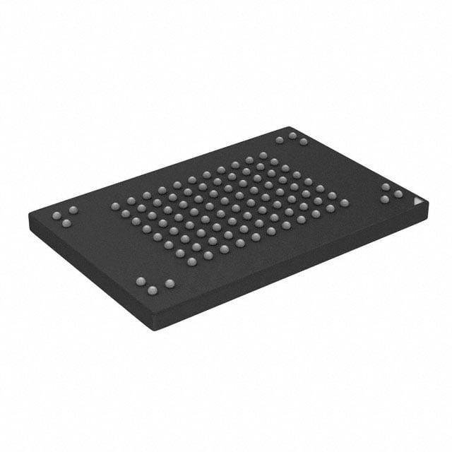
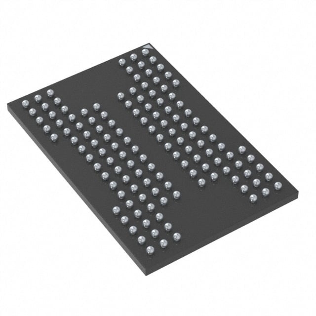
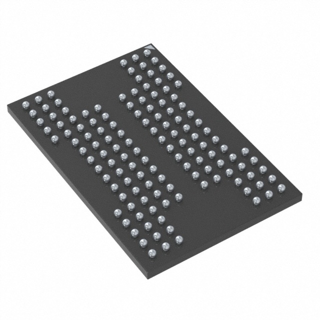
IC FLASH 64GBIT PAR 132VBGA |
|---|---|
| Quantity | 627 Available (as of June 17, 2026) |

| Product Category | Flash Memory |
|---|---|
| Manufacturer | Micron Technology Inc. |
| Manufacturing Status | Obsolete |
| Manufacturer Standard Lead Time | Contact Us |
| Datasheet |
Specifications & Environmental
| Device Package | 132-VBGA (12x18) | Memory Format | FLASH | Technology | FLASH - NAND | ||
|---|---|---|---|---|---|---|---|
| Memory Size | 64 Gbit | Access Time | N/A | Grade | Commercial | ||
| Clock Frequency | 100 MHz | Voltage | 2.7V ~ 3.6V | Memory Type | Non-Volatile | ||
| Operating Temperature | 0°C ~ 70°C (TA) | Write Cycle Time Word Page | N/A | Packaging | 132-VBGA | ||
| Mounting Method | Non-Volatile | Memory Interface | Parallel | Memory Organization | 8G x 8 | ||
| Moisture Sensitivity Level | 3 (168 Hours) | RoHS Compliance | ROHS3 Compliant | REACH Compliance | REACH Unknown | ||
| Qualification | N/A | ECCN | 3A991B1A | HTS Code | 8542.32.0071 |
Overview of MT29F64G08AECABJ1-10Z:A – IC FLASH 64GBIT PAR 132VBGA
The MT29F64G08AECABJ1-10Z:A is a 64 Gbit parallel NAND flash memory device implemented with single-level cell (SLC) technology. It is organized as 8G × 8 and supports both asynchronous and synchronous I/O with a parallel interface, targeting applications that require non-volatile storage with deterministic timing and robust endurance.
Key electrical and mechanical details include a 2.7 V–3.6 V supply range, a 100 MHz clock reference for synchronous modes, and a 132-ball VBGA (12 × 18) package. The device provides high per-pin throughput in synchronous mode (up to 200 MT/s per pin) and offers features for array management and status reporting suited to embedded storage designs.
Key Features
- Memory Core 64 Gbit NAND flash (8G × 8) implemented with SLC technology for program/erase endurance and predictable behavior.
- Interface Modes Supports both asynchronous and synchronous NAND I/O. Synchronous operation provides DDR timing (10 ns clock rate) and data strobe (DQS) signals for DQ synchronization.
- Performance Read/write throughput per pin: up to 200 MT/s in synchronous mode (DDR) and up to 50 MT/s in asynchronous mode; typical array timings include 35 µs read-page and 350 µs program-page.
- Memory Organization & Capacity Page size (×8): 8,640 bytes (8,192 + 448 bytes); block = 128 pages; device architecture includes 2 planes with block and plane addressing.
- Command & Advanced Functions Implements the ONFI 2.2-compliant protocol and advanced commands: program cache, read cache (sequential and random), multi-plane and multi-LUN operations, copyback, OTP mode, and read unique ID.
- Reliability & Endurance Endurance specified at 60,000 program/erase cycles and data retention compliant with JESD47G; operation-status byte is provided for software detection of completion and pass/fail conditions.
- Power & Voltage Operating VCC range: 2.7 V–3.6 V; VCCQ options include 1.7–1.95 V and 2.7–3.6 V for flexible I/O supply configurations.
- Package & Temperature Supplied in a 132-ball VBGA (12 × 18) package; commercial operating temperature range is 0 °C to +70 °C.
- Factory State & Reset The first block (block address 00h) is valid when shipped and a RESET (FFh) is required as the first command after power-on.
Typical Applications
- Embedded Storage Use as on-board non-volatile storage in systems that require parallel NAND flash memory with deterministic I/O and SLC endurance.
- Firmware and Boot Media Suitable for firmware storage and boot partitions where block/page organization and valid factory-shipped first block are useful.
- High‑Throughput Data Buffers Synchronous DDR-capable I/O and DQS support enable higher per-pin throughput for systems needing faster data transfer over a parallel NAND interface.
Unique Advantages
- Single‑Level Cell (SLC) Architecture: Provides predictable program/erase endurance and retention characteristics—specified at 60,000 P/E cycles and JESD47G-compliant retention.
- Dual I/O Modes: Supports both asynchronous and synchronous operation, giving designers flexibility to optimize for legacy parallel interfaces or higher-performance synchronous systems.
- ONFI 2.2 Compliance: Standardized NAND protocol and advanced command set simplify integration with controllers that support ONFI-compliant devices.
- Advanced Array Functions: Program/read caching, multi-plane and multi-LUN operations, and copyback reduce host-side control complexity and improve array efficiency.
- Flexible Supply Options: VCC and VCCQ supply ranges (2.7–3.6 V and 1.7–1.95 V / 2.7–3.6 V) allow adaptation to different system I/O voltage schemes.
- Compact BGA Package: 132-ball VBGA (12 × 18) enables dense board implementations while exposing the full parallel interface.
Why Choose MT29F64G08AECABJ1-10Z:A?
The MT29F64G08AECABJ1-10Z:A targets designs that need a 64 Gbit SLC NAND flash with both asynchronous and synchronous parallel interfaces, combining predictable endurance with options for higher per-pin throughput. Its ONFI 2.2 feature set, advanced array commands, and status reporting provide the controls needed for robust flash management in embedded systems.
This device is well suited for designs that require a compact 132-ball VBGA package, standard 2.7–3.6 V supply operation, and commercial temperature operation (0 °C to +70 °C). The specified endurance and JESD47G data-retention alignment support long-term data reliability in deployed systems.
Request a quote or submit an inquiry to receive pricing, availability, and lead-time information for the MT29F64G08AECABJ1-10Z:A.