MT46V16M16TG-75 IT:F
| Part Description |
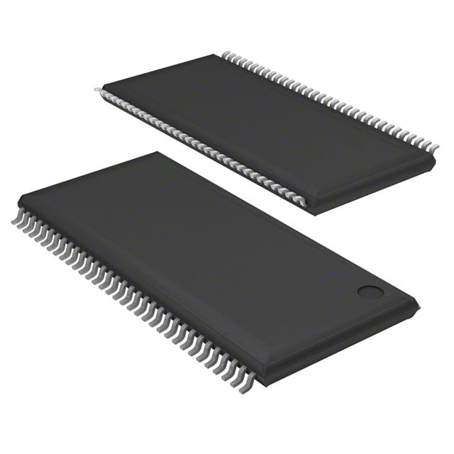
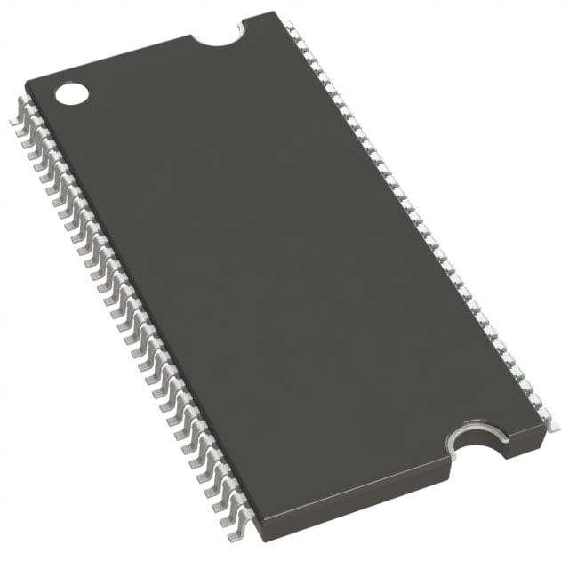
IC DRAM 256MBIT PARALLEL 66TSOP |
|---|---|
| Quantity | 324 Available (as of June 15, 2026) |

| Product Category | Memory |
|---|---|
| Manufacturer | Micron Technology Inc. |
| Manufacturing Status | Obsolete |
| Manufacturer Standard Lead Time | Contact Us |
| Datasheet |
Specifications & Environmental
| Device Package | 66-TSOP | Memory Format | DRAM | Technology | SDRAM - DDR | ||
|---|---|---|---|---|---|---|---|
| Memory Size | 256 Mbit | Access Time | 750 ps | Grade | Industrial | ||
| Clock Frequency | 133 MHz | Voltage | 2.3V ~ 2.7V | Memory Type | Volatile | ||
| Operating Temperature | -40°C ~ 85°C (TA) | Write Cycle Time Word Page | 15 ns | Packaging | 66-TSSOP (0.400", 10.16mm Width) | ||
| Mounting Method | Volatile | Memory Interface | Parallel | Memory Organization | 16M x 16 | ||
| Moisture Sensitivity Level | 2 (1 Year) | RoHS Compliance | RoHS non-compliant | REACH Compliance | REACH Unaffected | ||
| Qualification | N/A | ECCN | EAR99 | HTS Code | 8542.32.0024 |
Overview of MT46V16M16TG-75 IT:F – IC DRAM 256Mbit Parallel 66TSSOP
The MT46V16M16TG-75 IT:F is a 256Mbit DDR SDRAM organized as 16M x 16 with a parallel memory interface in a 66-TSSOP (0.400", 10.16mm width) package. It implements a pipelined double-data-rate architecture with source-synchronous data capture and supports industrial temperature operation.
Designed for systems requiring a parallel DDR memory device, the device provides 2.5V-class operation, programmable burst lengths, multiple internal banks for concurrent operation and timing options targeted to a 133 MHz clock rate.
Key Features
- Core Architecture Internal pipelined Double Data Rate (DDR) SDRAM architecture delivering two data accesses per clock cycle and a DLL to align DQ/DQS with CK.
- Memory Organization 256 Mbit capacity arranged as 16M × 16 with four internal banks (4 Meg × 16 × 4 banks).
- Performance & Timing Specified for a 133 MHz clock rate (speed grade -75/-6 variants include 133 MHz timing); access time listed as 750 ps and write cycle time (word page) of 15 ns. Programmable burst lengths of 2, 4, or 8.
- Data Strobe and Masking Bidirectional data strobe (DQS) transmitted/received with data for source-synchronous capture; x16 devices include two DQS signals (one per byte). Data mask (DM) support (x16 has two DMs, one per byte).
- Interface & Clocking Parallel memory interface with differential clock inputs (CK and CK#); commands entered on positive CK edge. DQS edge-aligned for READs and center-aligned for WRITEs.
- Power VDD supply range of 2.3 V to 2.7 V (nominal 2.5 V operation supported per datasheet options).
- Package & Mounting 66-pin TSSOP (66-TSSOP / 66-TSOP) package, longer-lead TSOP option (OCPL) noted for improved reliability; surface-mount mounting.
- Temperature Range Industrial temperature rating: –40°C to +85°C (TA).
- Refresh and Reliability Features Auto refresh and 8K refresh cycle support; self refresh options noted in datasheet (availability varies by option).
Unique Advantages
- Source-synchronous data capture: Bidirectional DQS with DLL alignment supports reliable timing between DQ and CK for DDR operation.
- Byte-level data control: Two DQS and two DM lines on x16 devices provide per-byte strobe and masking for flexible data handling.
- Industrial temperature rating: Specified operation from –40°C to +85°C supports deployment in temperature-challenging environments.
- Flexible timing and burst control: Programmable burst lengths (2, 4, 8) and multiple speed-grade timing options enable tuning for target system performance.
- 66-TSSOP package with longer leads option: TSOP package and OCPL longer-lead option are provided for board-level reliability considerations.
- Concurrent bank operation: Four internal banks allow overlapping operations to improve effective throughput within the DDR architecture.
Why Choose MT46V16M16TG-75 IT:F?
The MT46V16M16TG-75 IT:F provides a compact, industrial-temperature DDR SDRAM solution with a 16M × 16 organization and 256 Mbit capacity. Its source-synchronous DQS implementation, DLL alignment, and programmable burst lengths make it suitable where parallel DDR memory bandwidth and predictable timing are required.
With a 2.3–2.7 V supply range, 66-TSSOP packaging (with longer-lead OCPL option), and four internal banks for concurrent operation, this device is positioned for embedded and industrial systems that require a parallel DDR memory component from a recognized memory manufacturer.
If you would like pricing, availability, or a formal quote for MT46V16M16TG-75 IT:F, submit a request and our team will provide a quote and additional procurement information.