MT46V16M16TG-75:F
| Part Description |
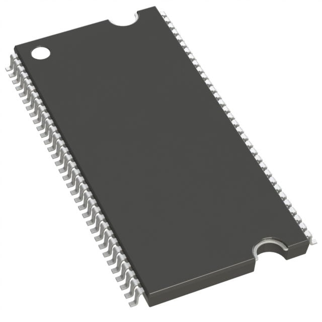
IC DRAM 256MBIT PARALLEL 66TSOP |
|---|---|
| Quantity | 1,282 Available (as of June 15, 2026) |

| Product Category | Memory |
|---|---|
| Manufacturer | Micron Technology Inc. |
| Manufacturing Status | Obsolete |
| Manufacturer Standard Lead Time | Contact Us |
| Datasheet |
Specifications & Environmental
| Device Package | 66-TSOP | Memory Format | DRAM | Technology | SDRAM - DDR | ||
|---|---|---|---|---|---|---|---|
| Memory Size | 256 Mbit | Access Time | 750 ps | Grade | Commercial | ||
| Clock Frequency | 133 MHz | Voltage | 2.3V ~ 2.7V | Memory Type | Volatile | ||
| Operating Temperature | 0°C ~ 70°C (TA) | Write Cycle Time Word Page | 15 ns | Packaging | 66-TSSOP (0.400", 10.16mm Width) | ||
| Mounting Method | Volatile | Memory Interface | Parallel | Memory Organization | 16M x 16 | ||
| Moisture Sensitivity Level | 2 (1 Year) | RoHS Compliance | N/A | REACH Compliance | REACH Unaffected | ||
| Qualification | N/A | ECCN | EAR99 | HTS Code | 8542.32.0024 |
Overview of MT46V16M16TG-75:F – IC DRAM 256MBIT PARALLEL 66TSOP
The MT46V16M16TG-75:F is a 256 Mbit DDR SDRAM device organized as 16M × 16 with a parallel memory interface in a 66-pin TSSOP package. It implements a pipelined double-data-rate architecture with two data accesses per clock cycle and is designed for systems requiring a 256 Mbit parallel DDR memory element operating at up to 133 MHz.
Key value is delivered through DDR performance (source-synchronous DQS), four internal banks for concurrent operation, and a compact 66‑TSSOP footprint for board-level integration in commercial-temperature (0°C to +70°C) applications.
Key Features
- Core Architecture Double Data Rate (DDR) SDRAM with internal pipelined DDR architecture; two data accesses per clock cycle and a DLL to align DQ/DQS with CK.
- Memory Organization 256 Mbit capacity implemented as 16M × 16 with four internal banks (4 Meg × 16 × 4 banks) to support concurrent bank operation.
- Performance & Timing Clock rate up to 133 MHz (speed grade -75), access time of 750 ps, and write cycle time (word page) of 15 ns. Programmable burst lengths of 2, 4, or 8.
- Data I/O and Signaling Source-synchronous data strobe (DQS) transmitted/received with data; x16 devices include two DQS signals (one per byte) and two data mask (DM) signals. Differential clock inputs (CK/CK#).
- Power VDD and VDDQ operating range centered on 2.5 V with specified supply range of 2.3 V to 2.7 V (VDD = +2.5 V ±0.2 V shown in device options).
- Package 66‑TSSOP (0.400", 10.16 mm width) plastic package for board-level mounting and integration.
- Operating Temperature Commercial temperature rating: 0°C to +70°C (TA).
Typical Applications
- Parallel DDR memory in system designs — Acts as a 256 Mbit DDR SDRAM component where parallel DDR memory is required, supporting 133 MHz operation.
- Banked memory architectures — Four internal banks and programmable burst lengths enable concurrent access patterns and burst transfers in designs that leverage bank interleaving.
- Board-level high-density memory — 16M × 16 organization provides 256 Mbit capacity in a compact 66‑TSSOP footprint for space-constrained PCBs.
Unique Advantages
- DDR source-synchronous capture: DQS transmitted and received with data (two DQS on x16) enables aligned read/write timing for reliable high-speed transfers.
- Concurrent bank operation: Four internal banks permit overlapping operations to improve effective throughput for bursty access patterns.
- Flexible burst and timing options: Programmable burst lengths (2, 4, 8) and defined speed-grade timing enable designers to match memory behavior to system timing requirements.
- Standard 2.5 V I/O: Device operates with VDD/VDDQ centered on 2.5 V (specified supply range 2.3 V–2.7 V), consistent with common DDR signaling requirements.
- Compact TSOP package: 66‑pin TSSOP (0.400" / 10.16 mm width) supports board-level integration where a slim, long-lead TSOP is desirable.
Why Choose MT46V16M16TG-75:F?
The MT46V16M16TG-75:F positions itself as a practical DDR SDRAM option where a 256 Mbit, 16‑bit parallel memory element is required. Its DDR pipelined architecture, source-synchronous DQS, four internal banks, and programmable burst lengths provide deterministic timing and flexibility for designs targeting 133 MHz operation.
Manufactured by Micron Technology, the device’s 66‑TSSOP package and commercial temperature rating (0°C to +70°C) make it suitable for board-level integration in systems that need compact, banked DDR memory with standard 2.5 V I/O signaling.
Request a quote or contact sales to discuss availability, pricing, and lead times for the MT46V16M16TG-75:F.