MT46V32M16P-6T:F TR
| Part Description |
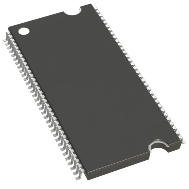
IC DRAM 512MBIT PAR 66TSOP |
|---|---|
| Quantity | 1,012 Available (as of June 15, 2026) |

| Product Category | Memory |
|---|---|
| Manufacturer | Micron Technology Inc. |
| Manufacturing Status | Obsolete |
| Manufacturer Standard Lead Time | Contact Us |
| Datasheet |
Specifications & Environmental
| Device Package | 66-TSOP | Memory Format | DRAM | Technology | SDRAM - DDR | ||
|---|---|---|---|---|---|---|---|
| Memory Size | 512 Mbit | Access Time | 700 ps | Grade | Commercial | ||
| Clock Frequency | 167 MHz | Voltage | 2.3V ~ 2.7V | Memory Type | Volatile | ||
| Operating Temperature | 0°C ~ 70°C (TA) | Write Cycle Time Word Page | 15 ns | Packaging | 66-TSSOP (0.400", 10.16mm Width) | ||
| Mounting Method | Volatile | Memory Interface | Parallel | Memory Organization | 32M x 16 | ||
| Moisture Sensitivity Level | 3 (168 Hours) | RoHS Compliance | ROHS Compliant | REACH Compliance | REACH Unaffected | ||
| Qualification | N/A | ECCN | EAR99 | HTS Code | 8542.32.0024 |
Overview of MT46V32M16P-6T:F TR – IC DRAM 512MBIT PAR 66TSOP
The MT46V32M16P-6T:F TR is a 512 Mbit double-data-rate (DDR) SDRAM organized as 32M × 16 with a parallel memory interface in a 66‑TSSOP (0.400", 10.16 mm width) package. It implements a pipelined DDR architecture with source‑synchronous data capture and on‑die DLL for aligned data timing.
This device targets designs that require 512 Mbit DDR memory density with byte‑wide (x16) data paths, delivering up to 167 MHz clock operation and support for programmable burst lengths, refresh modes and a range of timing grades for system memory applications.
Key Features
- Core / Architecture Internal pipelined DDR architecture providing two data accesses per clock cycle, differential clock inputs (CK/CK#) and an on‑die DLL to align DQ/DQS with CK.
- Memory Organization & Performance 512 Mbit capacity arranged as 32M × 16 with four internal banks; supports programmable burst lengths of 2, 4 or 8. Specified clock frequency up to 167 MHz and an access time of 700 ps.
- Data I/O and Timing Bidirectional data strobe (DQS) transmitted/received with data; x16 devices provide two DQS signals (one per byte). Device supports DQS edge‑alignment for READs and center‑alignment for WRITEs.
- Refresh and Power Management Auto refresh supported; self refresh is described in the device documentation (note: self refresh not available on AT devices as specified in the datasheet). Refresh count is 8K.
- Power Supply and I/O: VDD/VDDQ nominal 2.5 V with operating supply range 2.3 V to 2.7 V (SSTL_2 compatible I/O).
- Timing Grade and Performance Options Timing grade -6T corresponds to operation at the 167 MHz clock rate with defined data‑out and access windows per the timing table in the product documentation.
- Package & Temperature 66‑pin TSSOP (66‑TSOP) package with longer‑lead TSOP option noted for improved reliability. Commercial operating temperature range 0°C to +70°C.
- Write/Access Characteristics Write cycle time (word/page) specified at 15 ns and device timing parameters defined in the datasheet for CL and data‑out windows.
Typical Applications
- System memory for embedded platforms — Provides 512 Mbit DDR SDRAM capacity in designs requiring a parallel x16 data interface and standard commercial temperature operation.
- Memory expansion in legacy/board‑level designs — 66‑TSSOP package supports board layouts that use TSOP form factors for through‑board memory implementations.
- High‑throughput buffer memory — DDR architecture with programmable burst lengths and DQS‑aligned data capture suits buffering and burst transfer use cases within the supported clock range.
Unique Advantages
- DDR pipelined architecture: Two data accesses per clock cycle increase effective data throughput at the specified clock rates.
- Byte‑wise strobe and masking: Bidirectional DQS and dual data mask (DM) on x16 (one per byte) enable precise byte‑level timing and write masking.
- Flexible timing options: -6T timing grade supports operation at 167 MHz with defined data‑out and access windows for predictable timing design margins.
- SSTL_2 compatible I/O and 2.5 V nominal operation: Matches common DDR I/O signaling standards while supporting a 2.3 V to 2.7 V supply range for system integration.
- Package reliability option: Longer‑lead TSOP variant is offered for improved mechanical reliability in board mounting and handling.
- Comprehensive refresh and bank support: Four internal banks and 8K refresh count enable concurrent bank operation and established refresh management.
Why Choose MT46V32M16P-6T:F TR?
The MT46V32M16P-6T:F TR positions itself as a practical 512 Mbit DDR SDRAM option for designs that need a parallel x16 memory interface with defined timing characteristics up to 167 MHz. Its pipelined DDR architecture, DQS‑aligned capture and programmable burst lengths make it suitable where deterministic timing and burst transfers are required.
With a 66‑TSSOP package and commercial temperature rating, this device is appropriate for board‑level memory implementations that require 2.5 V nominal I/O signaling, four internal banks and standard refresh management. The documented timing grades and package options allow designers to match performance and mechanical requirements while relying on the referenced device specifications.
Request a quote or submit an RFQ to receive pricing, availability and lead‑time information for the MT46V32M16P-6T:F TR.