MT46V32M16TG-5B:F
| Part Description |
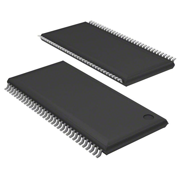
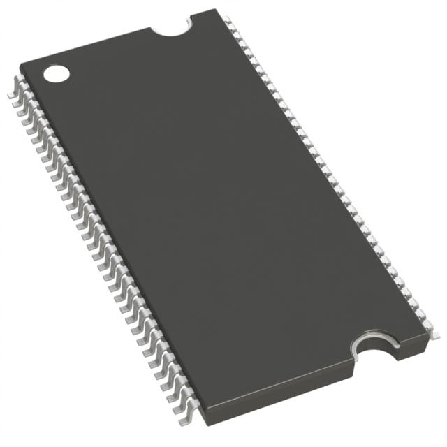
IC DRAM 512MBIT PARALLEL 66TSOP |
|---|---|
| Quantity | 1,254 Available (as of June 15, 2026) |
| Product Category | Memory |
|---|---|
| Manufacturer | Micron Technology Inc. |
| Manufacturing Status | Obsolete |
| Manufacturer Standard Lead Time | Contact Us |
| Datasheet |
Specifications & Environmental
| Device Package | 66-TSOP | Memory Format | DRAM | Technology | SDRAM - DDR | ||
|---|---|---|---|---|---|---|---|
| Memory Size | 512 Mbit | Access Time | 700 ps | Grade | Commercial | ||
| Clock Frequency | 200 MHz | Voltage | 2.5V ~ 2.7V | Memory Type | Volatile | ||
| Operating Temperature | 0°C ~ 70°C (TA) | Write Cycle Time Word Page | 15 ns | Packaging | 66-TSSOP (0.400", 10.16mm Width) | ||
| Mounting Method | Volatile | Memory Interface | Parallel | Memory Organization | 32M x 16 | ||
| Moisture Sensitivity Level | 3 (168 Hours) | RoHS Compliance | RoHS non-compliant | REACH Compliance | REACH Unaffected | ||
| Qualification | N/A | ECCN | EAR99 | HTS Code | 8542.32.0024 |
Overview of MT46V32M16TG-5B:F – IC DRAM 512MBIT PARALLEL 66TSOP
The MT46V32M16TG-5B:F is a 512 Mbit DDR SDRAM device in a 32M × 16 organization, provided in a 66‑pin TSSOP (66‑TSOP) package. It implements a double-data-rate architecture with source-synchronous data strobes and internal DLL, delivering two data accesses per clock cycle.
This device targets applications that require parallel DDR memory in a compact TSOP footprint, offering 200 MHz clock operation (DDR400 speed grade -5B), a 2.5 V I/O domain, and commercial temperature range operation (0°C to +70°C).
Key Features
- Memory core – 512 Mbit DDR SDRAM organized as 32M × 16 with four internal banks for concurrent operation.
- Double Data Rate (DDR) architecture – Internal pipelined DDR architecture enabling two data accesses per clock cycle; -5B timing grade supports up to 200 MHz clock rate.
- Data path and strobe – Bidirectional data strobe (DQS) transmitted/received with data; x16 implementation includes two DQS signals (one per byte) and two data mask (DM) signals.
- Clock and timing – Differential clock inputs (CK and CK#), DLL for aligning DQ/DQS transitions with CK, and programmable burst lengths of 2, 4, or 8.
- Refresh and self refresh – Auto refresh with 8192-cycle refresh; self refresh option available (not on AT devices as noted in the datasheet options).
- Electrical – VDD/VDDQ = 2.5 V ±0.2 V (or 2.6 V ±0.1 V for DDR400 option), SSTL_2 compatible I/O signaling.
- Performance timing – Access time listed as 700 ps; write cycle time (word/page) of 15 ns; data-out and access windows specified for the -5B speed grade.
- Package and thermal – 66‑TSSOP (0.400", 10.16 mm width) longer‑lead TSOP option for improved reliability; commercial temperature rating 0°C to +70°C.
Typical Applications
- Embedded memory subsystems – Provides 512 Mbit of volatile DDR storage in systems that require parallel DDR SDRAM with x16 data width.
- Board-level upgrades and legacy designs – 66‑pin TSOP package supports designs using TSSOP footprints where a compact, parallel DDR component is required.
- High-throughput buffering – DDR architecture and up to 200 MHz clocking support designs needing doubled data transfers per clock cycle for buffering and temporary storage.
Unique Advantages
- Double-data-rate throughput: Two data accesses per clock cycle increase effective bandwidth compared to single-data-rate devices.
- Byte-level strobe and mask: Two DQS and two DM signals on the x16 device provide per-byte data strobes and write masking for finer control of transfers.
- Flexible timing options: Programmable burst lengths (2, 4, 8) and defined speed grade (-5B) let designers optimize latency and burst behavior for target clock rates.
- SSTL_2 compatible signaling: 2.5 V I/O and differential clock inputs support standard DDR interface signaling for parallel memory buses.
- Compact TSOP package: 66‑TSSOP footprint with longer leads option (OCPL) for improved reliability in board-level implementations.
- Integrated refresh management: Auto refresh and self refresh support reduce external management overhead for maintaining data integrity in volatile memory.
Why Choose MT46V32M16TG-5B:F?
The MT46V32M16TG-5B:F combines a 32M × 16 DDR SDRAM organization with DDR-specific features—bidirectional DQS, DLL alignment, differential clocking, and programmable burst lengths—delivered in a compact 66‑TSSOP package. Its -5B timing grade supports 200 MHz clock operation, making it suitable for designs that require doubled data transfers per cycle while operating within a 2.5 V I/O domain and commercial temperature range.
This device is appropriate for designers specifying a parallel DDR memory solution in a TSOP footprint who need well-defined timing, refresh management, and byte-level strobe/mask capability. The combination of DDR architecture and standard electrical signaling provides a predictable, verifiable memory building block for board-level system memory designs.
Request a quote or submit a request for pricing and availability to obtain lead-time and quantity information for the MT46V32M16TG-5B:F.