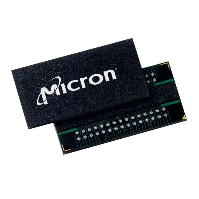
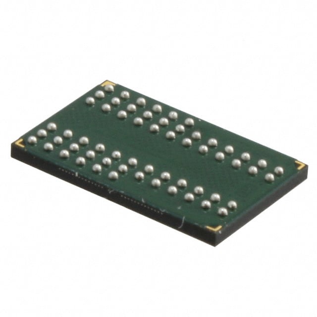
MT46V64M8CV-5B IT:J TR
| Part Description |
IC DRAM 512MBIT PARALLEL 60FBGA |
|---|---|
| Quantity | 627 Available (as of June 15, 2026) |

| Product Category | Memory |
|---|---|
| Manufacturer | Micron Technology Inc. |
| Manufacturing Status | Obsolete |
| Manufacturer Standard Lead Time | Contact Us |
| Datasheet |
Specifications & Environmental
| Device Package | 60-FBGA (8x12.5) | Memory Format | DRAM | Technology | SDRAM - DDR | ||
|---|---|---|---|---|---|---|---|
| Memory Size | 512 Mbit | Access Time | 700 ps | Grade | Industrial | ||
| Clock Frequency | 200 MHz | Voltage | 2.5V ~ 2.7V | Memory Type | Volatile | ||
| Operating Temperature | -40°C ~ 85°C (TA) | Write Cycle Time Word Page | 15 ns | Packaging | 60-TFBGA | ||
| Mounting Method | Volatile | Memory Interface | Parallel | Memory Organization | 64M x 8 | ||
| Moisture Sensitivity Level | 3 (168 Hours) | RoHS Compliance | ROHS3 Compliant | REACH Compliance | REACH Unknown | ||
| Qualification | N/A | ECCN | EAR99 | HTS Code | 8542.32.0028 |
Overview of MT46V64M8CV-5B IT:J TR – IC DRAM 512Mbit Parallel 60FBGA
The MT46V64M8CV-5B IT:J TR is a 512 Mbit DDR SDRAM (16M × 8 × 4 banks) in a 60-ball FBGA package, manufactured by Micron Technology Inc. It implements an internal pipelined double-data-rate architecture with source-synchronous data capture and differential clock inputs for high-throughput parallel memory operation.
This device targets designs that require a compact 60-ball FBGA memory solution operating from 2.5 V I/O and supporting up to a 200 MHz clock rate (DDR data rate), with industrial temperature range capability.
Key Features
- Core / Architecture Internal pipelined DDR architecture providing two data accesses per clock cycle; DLL aligns DQ and DQS transitions with CK for timing integrity.
- Memory Organization 64M × 8 configuration yielding 512 Mbit density with four internal banks to support concurrent operations and programmable burst lengths (2, 4, or 8).
- Interface & Timing Parallel DDR interface with bidirectional data strobe (DQS), differential clock inputs (CK/CK#), and command timing on positive CK edges; specified clock frequency up to 200 MHz and access time of 700 ps.
- Power & I/O VDD/VDDQ nominal operation at 2.5 V (specified 2.5 V ±0.2 V and option for 2.6 V ±0.1 V for DDR400); 2.5 V I/O compatible with SSTL_2 signaling.
- Package 60-ball FBGA (60-TFBGA / 60-FBGA, footprint 8 × 12.5 mm option) for compact board-level integration.
- Temperature Range Industrial operating temperature range: −40°C to +85°C (TA).
- Reliability & Maintenance Auto refresh and optional self refresh support; 8192 refresh cycles per 64 ms (commercial/industrial option).
- Write & Cycle Timing Write cycle time (word page) specified at 15 ns, supporting page-based write timing requirements.
Typical Applications
- Embedded memory for parallel-interface systems Provides 512 Mbit DDR SDRAM in a compact FBGA footprint for embedded designs requiring DDR performance and source-synchronous DQS signaling.
- Industrial-temperature electronics Suited for systems that must operate between −40°C and +85°C while maintaining DDR timing and refresh behavior.
- Board-level memory modules Ideal for PCB designs that need a 60-ball FBGA memory device with 2.5 V I/O and standard DDR command/timing interfaces.
Unique Advantages
- Double-data-rate throughput: Internal DDR architecture and DQS-based source-synchronous capture enable two data transfers per clock edge for increased bandwidth versus single-data-rate devices.
- Compact FBGA package: 60-ball FBGA (8 × 12.5 mm option) minimizes PCB area while providing a full parallel DDR interface for board-level integration.
- Industrial temperature support: Specified operation from −40°C to +85°C supports deployment in temperature-challenging environments without derating device specifications.
- SSTL_2 compatible I/O: 2.5 V I/O levels align with SSTL_2 signaling standards (VDD/VDDQ nominal 2.5 V), simplifying interface design with compatible controllers.
- Flexible burst and bank operation: Four internal banks and programmable burst lengths (2/4/8) enable efficient burst transfers and concurrent bank activity for optimized throughput.
- Timing control features: Differential clock inputs, DLL alignment, and DQS timing options help maintain predictable data timing and capture windows.
Why Choose IC DRAM 512MBIT PARALLEL 60FBGA?
The MT46V64M8CV-5B IT:J TR is positioned for designs requiring a 512 Mbit DDR SDRAM with industrial temperature capability, compact 60-ball FBGA packaging, and standard 2.5 V I/O. Its DDR architecture, onboard DLL, and source-synchronous DQS support predictable timing and reliable data transfer in parallel-interface systems.
This device is appropriate for engineers specifying board-level DDR memory where compact footprint, industrial temperature range, and established DDR timing features are required. Selecting this Micron-manufactured device provides a clear specification set for integration, timing closure, and thermal margin planning.
Request a quote or submit a pricing inquiry for MT46V64M8CV-5B IT:J TR to obtain lead-time, availability, and volume pricing information.