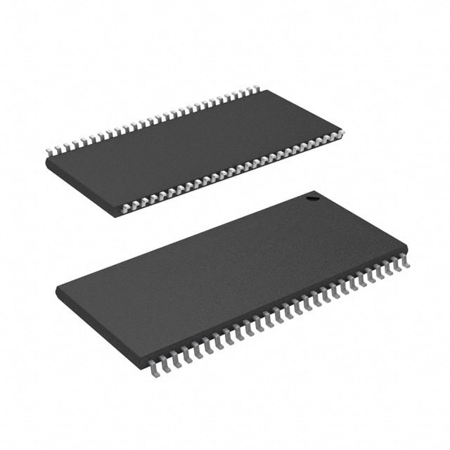
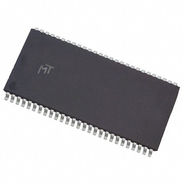
MT48LC16M16A2P-7E:D
| Part Description |
IC DRAM 256MBIT PAR 54TSOP II |
|---|---|
| Quantity | 40 Available (as of June 15, 2026) |

| Product Category | Memory |
|---|---|
| Manufacturer | Micron Technology Inc. |
| Manufacturing Status | Obsolete |
| Manufacturer Standard Lead Time | Contact Us |
| Datasheet |
Specifications & Environmental
| Device Package | 54-TSOP II | Memory Format | DRAM | Technology | SDRAM | ||
|---|---|---|---|---|---|---|---|
| Memory Size | 256 Mbit | Access Time | 5.4 ns | Grade | Commercial | ||
| Clock Frequency | 133 MHz | Voltage | 3V ~ 3.6V | Memory Type | Volatile | ||
| Operating Temperature | 0°C ~ 70°C (TA) | Write Cycle Time Word Page | 14 ns | Packaging | 54-TSOP (0.400", 10.16mm Width) | ||
| Mounting Method | Volatile | Memory Interface | Parallel | Memory Organization | 16M x 16 | ||
| Moisture Sensitivity Level | 3 (168 Hours) | RoHS Compliance | ROHS3 Compliant | REACH Compliance | REACH Unaffected | ||
| Qualification | N/A | ECCN | EAR99 | HTS Code | 8542.32.0024 |
Overview of MT48LC16M16A2P-7E:D – IC DRAM 256MBIT PAR 54TSOP II
The MT48LC16M16A2P-7E:D is a 256 Mbit synchronous DRAM (SDRAM) device organized as 16M × 16 with a parallel memory interface in a 54‑pin TSOP II (400 mil) package. It implements fully synchronous, pipelined SDRAM architecture and is provided by Micron Technology Inc.
Designed for PC100/PC133-class systems, this device operates at a clock frequency of 133 MHz with a voltage supply range of 3.0 V to 3.6 V and an operating temperature range of 0 °C to 70 °C, offering compact package integration for commercial applications.
Key Features
- Memory Architecture 256 Mbit SDRAM organized as 16M × 16 with four internal banks to improve access concurrency and hide row access/precharge.
- Synchronous, Pipelined Operation Fully synchronous device with all signals registered on the positive edge of the system clock and internal pipelining for column-address changes each clock cycle.
- Performance & Timing PC100- and PC133-compliant operation at a clock frequency of 133 MHz; the -7E speed grade targets 2-2-2 timing (RCD-RP-CL) and the product data lists an access time of 5.4 ns.
- Burst and Refresh Features Programmable burst lengths (1, 2, 4, 8, or full page), auto precharge, auto refresh and a standard 64 ms/8,192-cycle refresh scheme documented in the datasheet.
- Power and I/O Single-supply operation with 3.3 V nominal (3.0 V to 3.6 V) and LVTTL-compatible inputs and outputs for standard 3.3 V system interfacing.
- Package and Thermal 54‑pin TSOP II (0.400", 10.16 mm width) plastic package suitable for compact board layouts; commercial operating temperature range of 0 °C to 70 °C.
Typical Applications
- PC Memory Subsystems Use in PC100/PC133-class memory modules or systems requiring PC100/PC133-compliant SDRAM.
- Embedded System DRAM Integration where a 256 Mbit parallel SDRAM in a 54‑pin TSOP II footprint is required for system memory expansion.
- Legacy and Industrial Equipment (Commercial Range) Replacement or support for commercial-temperature electronics needing synchronous DRAM with a 3.3 V single-supply interface.
Unique Advantages
- Synchronous, pipelined design: Enables column address changes every clock cycle to support high-throughput burst access patterns.
- PC100/PC133 compliance: Matches timing classes commonly used in PC-oriented designs for compatibility with established system timings.
- Flexible burst control and internal banks: Programmable burst lengths and four internal banks help optimize sequential and random access performance.
- Compact TSOP II footprint: 54‑pin 400 mil package provides a small board-area solution for systems constrained by space.
- Standard 3.3 V I/O and LVTTL compatibility: Simplifies integration into 3.3 V systems and reduces interface translation requirements.
Why Choose IC DRAM 256MBIT PAR 54TSOP II?
The MT48LC16M16A2P-7E:D offers a verified Micron SDRAM solution with PC100/PC133-class synchronous operation, a 16M × 16 organization, and flexible burst and refresh features useful in a range of commercial embedded and system memory applications. Its 54‑pin TSOP II package and 3.0 V–3.6 V supply range suit compact boards that require standard 3.3 V SDRAM interfacing.
This device is appropriate for designers and procurement teams seeking a proven, standards‑aligned SDRAM component from an established memory manufacturer for commercial-temperature designs where 256 Mbit density, parallel interface, and 133 MHz clock operation are required.
Request a quote or submit a parts inquiry to obtain pricing, availability, and ordering information for the MT48LC16M16A2P-7E:D.