MT48LC32M8A2TG-75:D TR
| Part Description |
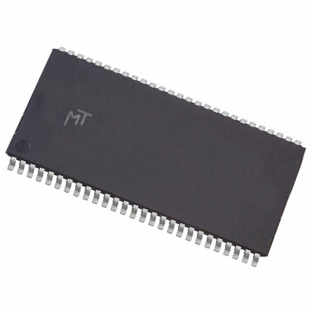
IC DRAM 256MBIT PAR 54TSOP II |
|---|---|
| Quantity | 711 Available (as of June 15, 2026) |

| Product Category | Memory |
|---|---|
| Manufacturer | Micron Technology Inc. |
| Manufacturing Status | Obsolete |
| Manufacturer Standard Lead Time | Contact Us |
| Datasheet |
Specifications & Environmental
| Device Package | 54-TSOP II | Memory Format | DRAM | Technology | SDRAM | ||
|---|---|---|---|---|---|---|---|
| Memory Size | 256 Mbit | Access Time | 5.4 ns | Grade | Commercial | ||
| Clock Frequency | 133 MHz | Voltage | 3V ~ 3.6V | Memory Type | Volatile | ||
| Operating Temperature | 0°C ~ 70°C (TA) | Write Cycle Time Word Page | 15 ns | Packaging | 54-TSOP (0.400", 10.16mm Width) | ||
| Mounting Method | Volatile | Memory Interface | Parallel | Memory Organization | 32M x 8 | ||
| Moisture Sensitivity Level | 3 (168 Hours) | RoHS Compliance | RoHS non-compliant | REACH Compliance | REACH Unaffected | ||
| Qualification | N/A | ECCN | EAR99 | HTS Code | 8542.32.0024 |
Overview of MT48LC32M8A2TG-75:D TR – IC DRAM 256Mbit PAR 54TSOP II
The MT48LC32M8A2TG-75:D TR is a 256 Mbit SDR SDRAM organized as 32M × 8 with a parallel memory interface. It is a fully synchronous DRAM designed for PC100- and PC133-compliant systems and supports pipelined operation with internal bank management for improved access concurrency.
This device operates from a single 3.3 V supply (3.0 V to 3.6 V), targets commercial operating temperatures (0°C to +70°C), and is delivered in a 54-pin TSOP II (0.400", 10.16 mm width) package for board-level mounting.
Key Features
- Core Memory Architecture 32M × 8 organization with 4 internal banks enabling concurrent bank access and row-precharge hiding.
- SDR SDRAM Functionality Fully synchronous operation with all signals registered on the positive edge of the system clock; internal pipelined operation supports column address changes every clock cycle.
- Performance PC100- and PC133-compliant timing with a clock frequency of 133 MHz for the -75 speed grade and an access time specified at 5.4 ns.
- Programmable Burst and Refresh Programmable burst lengths (1, 2, 4, 8, or full page) plus auto refresh and self-refresh support; 8192-cycle refresh intervals documented.
- Power Single 3.3 V ±0.3 V supply (3.0 V to 3.6 V) for system compatibility with standard 3.3 V logic levels.
- Package and Mounting Supplied in a 54-pin TSOP II (400 mil) plastic package suitable for surface mounting and compact board layouts.
- System Interfaces LVTTL-compatible inputs and outputs with parallel memory interface and standard SDRAM control signals.
- Timing Options Available timing grades include -75 (133 MHz, 3-3-3) and other documented grades; write cycle time (word/page) specified at 15 ns.
Typical Applications
- PC100/PC133 Memory Subsystems Use as system SDRAM in designs requiring PC100- or PC133-compliant synchronous DRAM.
- Board-Level Memory Expansion Implement memory expansion where a 54-pin TSOP II footprint and 32M × 8 organization are required.
- Embedded Systems with 3.3 V Supply Suitable for embedded applications that operate from a 3.0 V–3.6 V supply and require synchronous parallel DRAM.
Unique Advantages
- PC100/PC133 Compliance: Documented compliance with PC100 and PC133 timing grades simplifies integration into systems targeting those standards.
- Flexible Burst Control: Programmable burst lengths (1, 2, 4, 8, full page) enable tuning of burst behavior to match system memory access patterns.
- Internal Bank Architecture: Four internal banks provide hardware-level concurrency for improved effective throughput on sequential and interleaved accesses.
- Standard 54-pin TSOP II Package: Industry-standard TSOP II packaging supports compact board layouts and established assembly flows.
- Single 3.3 V Supply: Operation from a single 3.3 V supply (3.0 V–3.6 V) aligns with common system power rails for straightforward power design.
- Auto and Self-Refresh Options: Built-in auto refresh and self-refresh modes (per device options) reduce system refresh management overhead.
Why Choose MT48LC32M8A2TG-75:D TR?
The MT48LC32M8A2TG-75:D TR delivers a compact, 256 Mbit SDR SDRAM solution with a 32M × 8 organization and PC100/PC133-compliant timing, packaged in a 54-pin TSOP II footprint. Its internal bank structure, programmable burst lengths, and standard 3.3 V operation make it suitable for designs that require synchronous parallel DRAM with predictable timing characteristics.
This device is targeted at designers needing a board-mountable SDRAM option within a commercial temperature range (0°C to +70°C), offering timing grade choices and documented refresh and timing parameters to support system-level memory design and validation.
Request a quote or submit a pricing inquiry to evaluate MT48LC32M8A2TG-75:D TR for your next design or production project.