MT48LC4M16A2B4-7E:J TR
| Part Description |
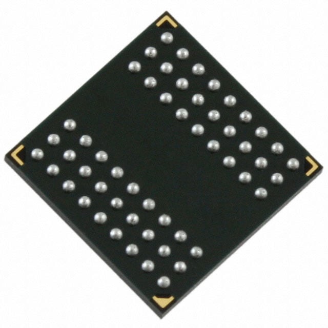
IC DRAM 64MBIT PARALLEL 54VFBGA |
|---|---|
| Quantity | 923 Available (as of June 15, 2026) |

| Product Category | Memory |
|---|---|
| Manufacturer | Micron Technology Inc. |
| Manufacturing Status | Obsolete |
| Manufacturer Standard Lead Time | Contact Us |
| Datasheet |
Specifications & Environmental
| Device Package | 54-VFBGA (8x8) | Memory Format | DRAM | Technology | SDRAM | ||
|---|---|---|---|---|---|---|---|
| Memory Size | 64 Mbit | Access Time | 5.4 ns | Grade | Commercial | ||
| Clock Frequency | 133 MHz | Voltage | 3V ~ 3.6V | Memory Type | Volatile | ||
| Operating Temperature | 0°C ~ 70°C (TA) | Write Cycle Time Word Page | 14 ns | Packaging | 54-VFBGA | ||
| Mounting Method | Volatile | Memory Interface | Parallel | Memory Organization | 4M x 16 | ||
| Moisture Sensitivity Level | 3 (168 Hours) | RoHS Compliance | ROHS Compliant | REACH Compliance | REACH Unaffected | ||
| Qualification | N/A | ECCN | EAR99 | HTS Code | 8542.32.0002 |
Overview of MT48LC4M16A2B4-7E:J TR – IC DRAM 64Mbit Parallel 54-VFBGA
The MT48LC4M16A2B4-7E:J TR is a 64 Mbit volatile SDRAM organized as 4M × 16 with a parallel memory interface. It implements synchronous SDRAM architecture with internal pipelined operation and banked memory for efficient row/column access.
Targeted at designs that require a compact, parallel SDRAM device, this part offers PC100/PC133-compliant operation, a 133 MHz clock capability, and a 54-ball VFBGA (8 × 8 mm) package for board-level memory integration.
Key Features
- Memory Architecture 64 Mbit SDRAM organized as 4M × 16 with internal banks to optimize row access and precharge sequencing.
- SDR SDRAM Core Fully synchronous operation with all signals registered on the positive edge of the system clock and internal pipelined operation allowing column address changes every clock cycle.
- Performance 133 MHz clock frequency with an access time of 5.4 ns and a word page write cycle time of 14 ns for timing-sensitive designs.
- Timing Options PC100- and PC133-compliant timing; datasheet lists programmable CAS/read latency and burst lengths (BL = 1, 2, 4, 8, or full page).
- Refresh and Power Modes Auto refresh and self refresh modes are supported (standard and low-power modes noted in the datasheet; low-power not available on AT devices).
- Interface and I/O Parallel memory interface with LVTTL-compatible inputs and outputs for system-level signaling compatibility.
- Power Single-supply operation from 3.0 V to 3.6 V (3.3 V ±0.3 V as specified in the datasheet).
- Package and Temperature 54-ball VFBGA (8 × 8 mm) package; commercial operating temperature range of 0°C to +70°C (TA).
Typical Applications
- Parallel Memory Systems — Fits board-level designs that require a compact, parallel SDRAM device with 64 Mbit capacity and PC100/PC133 timing.
- Embedded Boards — Provides synchronous DRAM storage for embedded systems needing a 4M × 16 memory organization in a small VFBGA footprint.
- Timing-Critical Designs — Suited for applications that require defined access time and write cycle timing (5.4 ns access time, 14 ns word-page write cycle).
Unique Advantages
- Compact VFBGA Package: 54-ball VFBGA (8 × 8 mm) minimizes PCB area for space-constrained designs.
- Industry Timing Compliance: PC100 and PC133 timing compatibility simplifies integration with systems designed to those clock standards.
- Flexible Burst and Bank Management: Programmable burst lengths and internal banks enable efficient data transfer patterns and hidden row access.
- Standard Voltage Range: Operates from 3.0 V to 3.6 V, matching common 3.3 V system rails for straightforward power integration.
- Deterministic Performance: Documented access time (5.4 ns) and write-cycle timing (14 ns) support predictable memory timing analysis.
Why Choose MT48LC4M16A2B4-7E:J TR?
The MT48LC4M16A2B4-7E:J TR provides a compact, parallel SDRAM solution with PC100/PC133-compliant timing, a 4M × 16 memory organization, and documented performance figures (133 MHz clock, 5.4 ns access time). Its 54-ball VFBGA package and 3.0–3.6 V supply range make it suitable for board-level memory integration where footprint and timing predictability matter.
This device is appropriate for designers needing a verified SDRAM component with programmable burst behavior, internal bank management, and standard refresh/power modes as specified in the datasheet. Its specification set supports practical deployment in systems that require a 64 Mbit parallel SDRAM element within a commercial temperature range.
Request a quote or submit an inquiry for pricing and availability of the MT48LC4M16A2B4-7E:J TR. Our team can provide lead-time and ordering information to support your design schedules.