MT48LC4M16A2B4-7E:J
| Part Description |
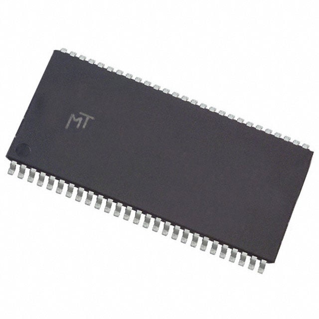
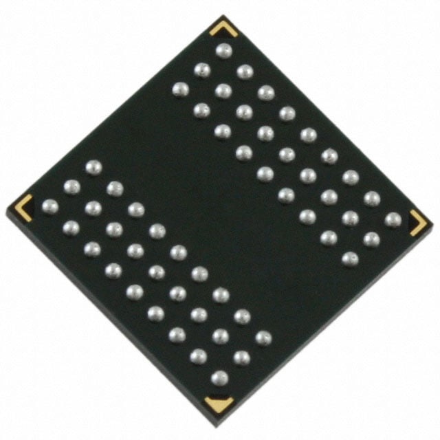
IC DRAM 64MBIT PARALLEL 54VFBGA |
|---|---|
| Quantity | 155 Available (as of June 9, 2026) |

| Product Category | Memory |
|---|---|
| Manufacturer | Micron Technology Inc. |
| Manufacturing Status | Obsolete |
| Manufacturer Standard Lead Time | Contact Us |
| Datasheet |
Specifications & Environmental
| Device Package | 54-VFBGA (8x8) | Memory Format | DRAM | Technology | SDRAM | ||
|---|---|---|---|---|---|---|---|
| Memory Size | 64 Mbit | Access Time | 5.4 ns | Grade | Commercial | ||
| Clock Frequency | 133 MHz | Voltage | 3V ~ 3.6V | Memory Type | Volatile | ||
| Operating Temperature | 0°C ~ 70°C (TA) | Write Cycle Time Word Page | 14 ns | Packaging | 54-VFBGA | ||
| Mounting Method | Volatile | Memory Interface | Parallel | Memory Organization | 4M x 16 | ||
| Moisture Sensitivity Level | 3 (168 Hours) | RoHS Compliance | ROHS3 Compliant | REACH Compliance | REACH Unaffected | ||
| Qualification | N/A | ECCN | EAR99 | HTS Code | 8542.32.0002 |
Overview of MT48LC4M16A2B4-7E:J – IC DRAM 64MBIT PARALLEL 54VFBGA
The MT48LC4M16A2B4-7E:J is a 64 Mbit volatile SDRAM organized as 4M × 16 with a parallel memory interface in a 54-ball VFBGA (8×8) package. It implements fully synchronous SDRAM architecture with internal banks and pipelined operation for predictable, clocked memory access.
Designed for commercial-grade systems, the device operates at a 133 MHz clock frequency, supports a 3.0–3.6 V supply range, and is specified for an ambient operating temperature of 0°C to 70°C, making it suitable for board-level designs that require compact, parallel SDRAM memory.
Key Features
- Memory Architecture 64 Mbit SDRAM organized as 4M × 16 with multiple internal banks to hide row access/precharge and enable pipelined operation.
- Synchronous Operation Fully synchronous SDRAM with all signals registered on the positive edge of the system clock; column address can be changed every clock cycle.
- Performance 133 MHz clock frequency with an access time of 5.4 ns (product data) and a write cycle time (word page) of 14 ns.
- Burst and Refresh Features Programmable burst lengths (1, 2, 4, 8 or full page), auto precharge and auto refresh, plus self-refresh modes as documented in the datasheet.
- Standards Compliance PC100- and PC133-compliant timing options are listed in the product datasheet to support common SDRAM timing profiles.
- Power Single 3.0–3.6 V supply (3.3 V ±0.3 V per datasheet) for integration into standard 3.3 V systems.
- Package and Mounting 54-ball VFBGA (8×8) package for compact, board-level mounting with a parallel interface.
- Temperature Range Commercial operating ambient range 0°C to 70°C.
Typical Applications
- Commercial Electronics — System memory in commercial-grade products that require a compact parallel SDRAM solution within the 0°C to 70°C operating range.
- Embedded Systems — Board-level memory for embedded designs that use synchronous parallel DRAM and require 64 Mbit density at 133 MHz operation.
- Legacy Parallel-Memory Designs — Replacement or upgrade memory for systems designed around parallel SDRAM architectures.
- Space-Constrained PCBs — Compact 54-ball VFBGA (8×8) package suited to high-density layouts.
Unique Advantages
- Compact VFBGA package: 54-ball 8×8 VFBGA minimizes board footprint while providing parallel memory connectivity.
- Synchronous, pipelined architecture: Internal banks and pipelined operation allow column address updates every clock cycle for efficient memory throughput.
- Flexible timing and burst control: Programmable burst lengths and PC100/PC133 timing options enable designers to balance throughput and latency.
- Robust power tolerance: 3.0–3.6 V supply range (3.3 V ±0.3 V) supports typical 3.3 V system margins.
- Commercial-grade specification: Specified for 0°C to 70°C operation for deployments in commercial environments.
Why Choose MT48LC4M16A2B4-7E:J?
The MT48LC4M16A2B4-7E:J delivers a mid-density, parallel SDRAM option with synchronous, pipelined operation and internal bank architecture from Micron Technology, Inc. Its 4M × 16 organization, 133 MHz clocking, and compact 54-ball VFBGA package make it suitable for board-level designs that require a reliable, space-efficient parallel memory solution.
For designers targeting commercial systems that need predictable synchronous memory behavior, programmable burst control, and standard 3.3 V supply compatibility, this device provides a documented feature set and timing options referenced in the product datasheet.
Request a quote or submit a pricing and availability inquiry for the MT48LC4M16A2B4-7E:J to discuss lead times and volume support.