MT48LC4M32B2P-6A AAT:L
| Part Description |
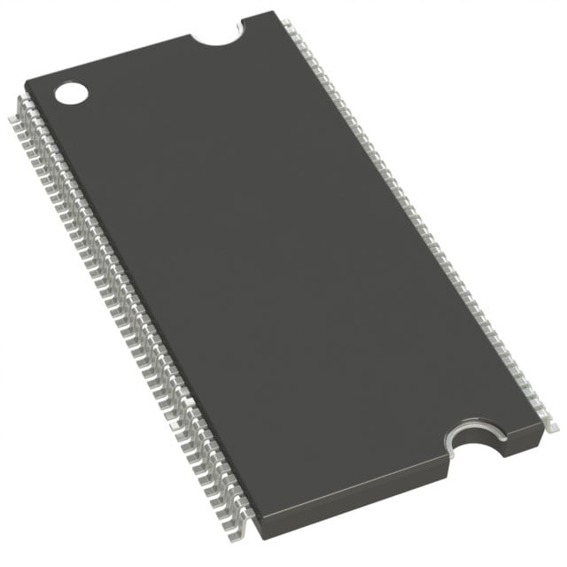
IC DRAM 128MBIT PAR 86TSOP II |
|---|---|
| Quantity | 174 Available (as of June 17, 2026) |

| Product Category | DRAM Memory |
|---|---|
| Manufacturer | Micron Technology Inc. |
| Manufacturing Status | Obsolete |
| Manufacturer Standard Lead Time | Contact Us |
| Datasheet |
Specifications & Environmental
| Device Package | 86-TSOP II | Memory Format | DRAM | Technology | SDRAM | ||
|---|---|---|---|---|---|---|---|
| Memory Size | 128 Mbit | Access Time | 5.4 ns | Grade | Automotive | ||
| Clock Frequency | 167 MHz | Voltage | 3V ~ 3.6V | Memory Type | Volatile | ||
| Operating Temperature | -40°C ~ 105°C (TA) | Write Cycle Time Word Page | 12 ns | Packaging | 86-TFSOP (0.400", 10.16mm Width) | ||
| Mounting Method | Volatile | Memory Interface | Parallel | Memory Organization | 4M x 32 | ||
| Moisture Sensitivity Level | 3 (168 Hours) | RoHS Compliance | ROHS3 Compliant | REACH Compliance | REACH Unaffected | ||
| Qualification | AEC-Q100 | ECCN | 3A991B1A | HTS Code | 8542.32.0002 |
Overview of MT48LC4M32B2P-6A AAT:L – IC DRAM 128MBIT PAR 86TSOP II
The MT48LC4M32B2P-6A AAT:L is a 128 Mbit (4M x 32) synchronous DRAM (SDRAM) device in a 86-pin TSOP II (0.400", 10.16 mm width) package. It provides a parallel memory interface with pipelined, fully synchronous operation and is offered in an automotive-grade variant with AEC-Q100 qualification.
Designed for systems that require a 3.3 V class SDRAM solution, the device targets embedded and automotive applications where defined timing, programmable burst modes and a wide operating temperature range are required.
Key Features
- Core Architecture — 4M × 32 organization (1 M × 32 × 4 banks) providing a total memory size of 128 Mbit with internal banks to hide row access and precharge.
- Synchronous SDRAM — Fully synchronous operation with all signals registered on the positive edge of the system clock and internal pipelined operation allowing column address changes every clock cycle.
- Performance — Clock frequency up to 167 MHz and an access time of 5.4 ns (specified); supports CAS latencies of 1, 2 and 3 for timing flexibility.
- Burst and Command Flexibility — Programmable burst lengths of 1, 2, 4, 8 or full page; supports auto precharge (including concurrent auto precharge), auto refresh and burst modes.
- Refresh Options — Auto refresh supported; datasheet documents refresh timing including automotive 16 ms/4,096-cycle refresh (3.9 µs/row).
- Electrical and I/O — LVTTL-compatible inputs and outputs; single supply voltage range of 3.0 V to 3.6 V (datasheet cites +3.3 V ±0.3 V).
- Thermal and Qualification — Automotive-grade device with AEC-Q100 qualification and an operating ambient temperature range of −40 °C to +105 °C (TA).
- Package — 86-pin TSOP II (400 mil) package, compact footprint with 10.16 mm width for space-constrained board layouts.
- Write and Cycle Timing — Write cycle (word page) timing of 12 ns; internal timing options documented in the datasheet for system integration.
- Self Refresh Note — Datasheet lists self refresh mode but notes that self refresh is not available on AT (automotive) devices; consult device documentation for variant-specific behavior.
Typical Applications
- Automotive electronics — Automotive-grade SDRAM for embedded controllers and modules requiring AEC-Q100 qualification and extended temperature operation.
- Embedded systems — Parallel SDRAM memory expansion for microcontroller- or processor-based designs needing synchronous, pipelined DRAM.
- Industrial control — Memory for industrial applications that require wide temperature range operation (−40 °C to +105 °C) and defined timing behavior.
- Legacy parallel memory interfaces — Drop-in SDRAM solution for systems using parallel DRAM interfaces and standard 3.3 V supply domains.
Unique Advantages
- Automotive-qualified component: AEC-Q100 qualification and a −40 °C to +105 °C operating range make the device suitable for automotive and harsh-environment designs that require validated components.
- Flexible timing and burst control: Support for CAS latencies 1–3 and programmable burst lengths allows designers to tune performance for specific access patterns and system clocking.
- High-speed synchronous operation: Up to 167 MHz clocking with internal pipelined operation and bank architecture enables efficient, predictable data throughput in synchronous systems.
- Standard supply compatibility: Operates from a 3.0 V to 3.6 V supply (documented as +3.3 V ±0.3 V), matching common system power rails and simplifying power design.
- Compact board-level footprint: 86-pin TSOP II (400 mil) package provides a space-efficient memory option for dense PCBs.
- Comprehensive datasheet detail: Detailed timing, command and package information in the datasheet supports rigorous system integration and validation.
Why Choose MT48LC4M32B2P-6A AAT:L?
The MT48LC4M32B2P-6A AAT:L combines a standard 3.3 V synchronous DRAM architecture with automotive-grade qualification and a compact TSOP II package, offering a practical memory building block for embedded and automotive systems. Its programmable burst modes, supported CAS latencies and pipelined internal operation provide predictable timing control for designers integrating parallel SDRAM.
This device is suited to engineers and procurement teams specifying robust, qualified SDRAM for applications that require defined timing performance, automotive qualification (AEC-Q100) and wide operating temperature support. Detailed datasheet coverage facilitates system-level timing integration and validation.
Request a quote or submit an RFQ to obtain pricing and availability for MT48LC4M32B2P-6A AAT:L. Provide your required quantities and lead-time constraints to receive a formal response.