MT48LC8M8A2TG-75:G TR
| Part Description |
IC DRAM 64MBIT PAR 54TSOP II |
|---|---|
| Quantity | 588 Available (as of June 15, 2026) |

| Product Category | Memory |
|---|---|
| Manufacturer | Micron Technology Inc. |
| Manufacturing Status | Obsolete |
| Manufacturer Standard Lead Time | Contact Us |
| Datasheet |
Specifications & Environmental
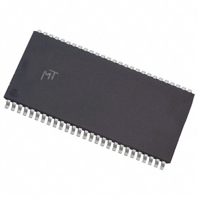
| Device Package | 54-TSOP II | Memory Format | DRAM | Technology | SDRAM | ||
|---|---|---|---|---|---|---|---|
| Memory Size | 64 Mbit | Access Time | 5.4 ns | Grade | Commercial | ||
| Clock Frequency | 133 MHz | Voltage | 3V ~ 3.6V | Memory Type | Volatile | ||
| Operating Temperature | 0°C ~ 70°C (TA) | Write Cycle Time Word Page | 15 ns | Packaging | 54-TSOP (0.400", 10.16mm Width) | ||
| Mounting Method | Volatile | Memory Interface | Parallel | Memory Organization | 8M x 8 | ||
| Moisture Sensitivity Level | 3 (168 Hours) | RoHS Compliance | RoHS non-compliant | REACH Compliance | REACH Unaffected | ||
| Qualification | N/A | ECCN | EAR99 | HTS Code | 8542.32.0002 |
Overview of MT48LC8M8A2TG-75:G TR – 64 Mbit SDRAM, 54‑pin TSOP II
The MT48LC8M8A2TG-75:G TR is a 64 Mbit synchronous DRAM (SDRAM) device organized as 8M x 8 with internal bank architecture. It provides a parallel memory interface in a 54-pin TSOP II (400 mil, 10.16 mm width) package and operates from a 3.0 V to 3.6 V supply.
Designed for systems requiring parallel SDRAM memory, this device supports PC66, PC100 and PC133 timing options and includes internal features to support pipelined operation, auto refresh and self-refresh modes.
Key Features
- Core / Architecture 64 Mbit SDRAM organized as 8M x 8 with internal bank structure (described as 2 Meg × 8 × 4 banks in the datasheet) to support internal banked access and hidden row access/precharge.
- Performance / Timing PC66-, PC100-, and PC133-compliant timing; specified clock frequency up to 133 MHz and an access time of 5.4 ns. The datasheet also lists a -75 timing option corresponding to 7.5 ns at CL = 3.
- Burst and Refresh Programmable burst lengths (1, 2, 4, 8, or full page), Auto Precharge (including concurrent auto precharge), Auto Refresh and Self Refresh modes with a 4,096-cycle refresh (64 ms) implementation.
- Interface / I/O Parallel memory interface with LVTTL-compatible inputs and outputs and support for internal pipelined operation allowing column address changes every clock cycle.
- Power Single +3.3 V ±0.3 V power supply range (3.0 V to 3.6 V) with standard and low-power self-refresh options documented in the datasheet.
- Package and Temperature 54-pin TSOP II (400 mil) plastic package with commercial operating temperature range 0 °C to +70 °C (TA).
- Write and Cycle Timing Write cycle timing and word/page write recovery parameters are provided; example specification shows write cycle time (word/page) at 15 ns in the product data.
Unique Advantages
- Flexible timing options: Support for PC66/PC100/PC133 timing and a documented -75 timing option (7.5 ns @ CL=3) enables selection of timing consistent with system clocking requirements.
- Banked memory architecture: Internal banks and pipelined operation help hide row access/precharge latency and allow column address changes every clock cycle for efficient burst transfers.
- Standard 3.3 V supply: Single +3.3 V ±0.3 V operation simplifies power supply design for systems using standard 3.3 V logic levels.
- Compact TSOP II package: 54-pin TSOP II (400 mil, 10.16 mm width) offers a space-efficient physical footprint for board-level integration.
- Robust refresh and low-power modes: Auto Refresh, Auto Precharge and Self Refresh modes (including low-power self-refresh) provide data retention options and power management flexibility.
Why Choose MT48LC8M8A2TG-75:G TR?
The MT48LC8M8A2TG-75:G TR delivers a practical 64 Mbit parallel SDRAM solution with PC133-capable timing, banked architecture for efficient pipelined operation, and programmable burst functionality. Its documented timing options, LVTTL I/O compatibility, and standard +3.3 V supply make it suitable for designs that require an off-the-shelf SDRAM device in a compact 54-pin TSOP II package.
This part is well suited to engineers specifying parallel SDRAM memory where clear timing, refresh behavior, and package dimensions are required. The provided datasheet details timing options, refresh behavior and package pin assignments to support integration and validation in target systems.
Request a quote or contact sales to discuss pricing, availability and technical questions about MT48LC8M8A2TG-75:G TR.