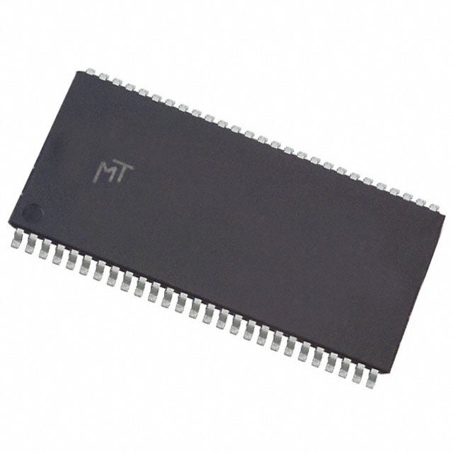
MT49H16M16FM-5 TR
| Part Description |
IC DRAM 256MBIT PARALLEL 144UBGA |
|---|---|
| Quantity | 812 Available (as of June 15, 2026) |
| Product Category | Memory |
|---|---|
| Manufacturer | Micron Technology Inc. |
| Manufacturing Status | Obsolete |
| Manufacturer Standard Lead Time | Contact Us |
| Datasheet |
Specifications & Environmental
| Device Package | 144-�BGA (18.5x11) | Memory Format | DRAM | Technology | DRAM | ||
|---|---|---|---|---|---|---|---|
| Memory Size | 256 Mbit | Access Time | N/A | Grade | Extended / Automotive-like | ||
| Clock Frequency | 200 MHz | Voltage | 1.7V ~ 1.95V | Memory Type | Volatile | ||
| Operating Temperature | 0°C ~ 95°C (TC) | Write Cycle Time Word Page | N/A | Packaging | 144-TFBGA | ||
| Mounting Method | Volatile | Memory Interface | Parallel | Memory Organization | 16M x 16 | ||
| Moisture Sensitivity Level | 3 (168 Hours) | RoHS Compliance | ROHS3 Compliant | REACH Compliance | REACH Unaffected | ||
| Qualification | N/A | ECCN | EAR99 | HTS Code | 8542.32.0036 |
Overview of MT49H16M16FM-5 TR – 256Mbit Parallel DRAM, 144 μBGA
The MT49H16M16FM-5 TR is a 256 Mbit Reduced Latency DRAM (RLDRAM®) device in a parallel 16‑bit organization (16M × 16) provided in a 144‑ball μBGA package. It implements an RLDRAM architecture with 8 internal banks, non‑multiplexed addresses and DDR data transfers to support fast random access and high bandwidth data paths.
Designed for telecommunications, networking and cache-type data storage applications, this device delivers programmable read latency, per‑pin high data rates and a compact BGA package suitable for space‑constrained high‑performance designs.
Key Features
- Memory Organization – 16M × 16 configuration providing 256 Mbit capacity with eight internal banks for concurrent access and cyclic bank addressing to maximize bandwidth.
- Reduced Latency RLDRAM Architecture – RLDRAM design with non‑multiplexed addresses and internal auto precharge for optimized fast random access and predictable latency.
- High Data Rate – Supports up to 600 Mb/sec per pin data rate and double data rate (DDR) transfers with non‑interruptible sequential bursts and 2‑ or 4‑bit prefetch modes.
- Programmable Read Latency – READ latency (RL) is programmable (RL = 5–6) to tune timing for specific system requirements.
- Interface & I/O – Parallel 16‑bit interface with data valid (DVLD), data mask signals (DM0/DM1), and differential echo clock; pseudo‑HSTL 1.8V I/O supply and 1.8V VDDQ signaling options are supported.
- Voltage & Power – Device supply ranges include 1.7 V to 1.95 V; datasheet references VEXT = 2.5 V with VDD and VDDQ at 1.8 V.
- Package – 144‑ball μBGA package (11 mm × 18.5 mm) in a compact footprint (144‑µBGA, 18.5 × 11 mm) for dense board layouts.
- Operating Temperature – Case temperature range 0 °C to 95 °C (T_C) for commercial thermal environments.
- System & Test – IEEE 1149.1 JTAG boundary scan support and defined refresh requirements (32 ms at 95 °C case temperature; 8K refresh per bank, 64K refresh total per 32 ms) for system integration and testability.
Typical Applications
- Telecommunications equipment – High‑bandwidth data buffering and fast random access storage for packet and frame processing.
- Networking systems – Per‑port buffering, queue management and cache functions in switches, routers and line cards.
- Cache memory – Low‑latency cache or scratch memory in communication and high‑speed processing subsystems.
Unique Advantages
- Reduced access latency: RLDRAM architecture and non‑multiplexed addresses cut access overhead compared with multiplexed DRAM approaches, improving random access performance.
- High per‑pin bandwidth: Support for up to 600 Mb/sec per pin and DDR bursts enables sustained high throughput across the parallel interface.
- Tunable timing: Programmable READ latency (RL = 5–6) allows designers to align device timing with system controller requirements.
- Robust system features: DVLD, data mask signals and internal auto precharge simplify controller logic for write masking, read validation and transaction completion.
- Compact package: 144‑ball μBGA (11 mm × 18.5 mm) minimizes board area while providing the connectivity needed for high‑speed designs.
- Commercial temperature range: Rated for 0 °C to 95 °C case temperature to support a range of commercial networking and telecom deployments.
Why Choose IC DRAM 256MBIT PARALLEL 144UBGA?
The MT49H16M16FM-5 TR combines Micron’s RLDRAM architecture with a compact 144‑ball μBGA footprint to deliver a 256 Mbit, 16‑bit parallel memory optimized for fast random access and high bandwidth. Its programmable latency, high per‑pin data rates and system‑level features (DVLD, DM signals, JTAG) make it suitable for telecommunications, networking and cache applications where predictable low latency and throughput are important.
This device is suitable for designers seeking a purpose‑built RLDRAM solution for compact, high‑performance boards that require controlled timing, robust refresh behavior and a small package profile.
Request a quote or contact sales to discuss availability, pricing and technical support for the MT49H16M16FM-5 TR.