W25N512GVPIT
| Part Description |
IC FLASH 512MBIT SPI/QUAD 8WSON |
|---|---|
| Quantity | 754 Available (as of June 14, 2026) |

| Product Category | Memory |
|---|---|
| Manufacturer | Winbond Electronics |
| Manufacturing Status | Active |
| Manufacturer Standard Lead Time | 24 Weeks |
| Datasheet |
Specifications & Environmental
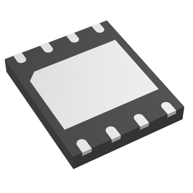
| Device Package | 8-WSON (6x5) | Memory Format | FLASH | Technology | FLASH - NAND (SLC) | ||
|---|---|---|---|---|---|---|---|
| Memory Size | 512 Mbit | Access Time | 7 ns | Grade | Industrial | ||
| Clock Frequency | 166 MHz | Voltage | 2.7V ~ 3.6V | Memory Type | Non-Volatile | ||
| Operating Temperature | -40°C ~ 85°C (TA) | Write Cycle Time Word Page | 700 μs | Packaging | 8-WDFN Exposed Pad | ||
| Mounting Method | Non-Volatile | Memory Interface | SPI - Quad I/O | Memory Organization | 64M x 8 | ||
| Moisture Sensitivity Level | 3 (168 Hours) | RoHS Compliance | ROHS3 Compliant | REACH Compliance | REACH Unaffected | ||
| Qualification | N/A | ECCN | 3A991B1A | HTS Code | 8542.32.0071 |
Overview of W25N512GVPIT – IC FLASH 512Mbit SPI/Quad 8WSON
The W25N512GVPIT is a 3V, 512 M-bit serial SLC NAND flash memory device implementing Dual/Quad SPI with buffer read and continuous read modes. It provides a 64M x 8 memory organization and is optimized for serial non-volatile storage in systems that require Quad I/O access.
Designed for integration in space-constrained designs, the device supports a clock frequency up to 166 MHz, operates from 2.7 V to 3.6 V, and is available in an 8-WSON (6×5 mm) package with an exposed pad. Operational temperature range is −40 °C to 85 °C.
Key Features
- Memory Technology 512 Mbit SLC NAND flash, organized as 64M × 8 for serial non-volatile storage.
- Interface & Performance Dual/Quad SPI interface (Quad I/O) with support for clock rates up to 166 MHz and an access time of 7 ns for fast serial read operations.
- Read Modes Buffer Read and Continuous Read modes are supported to optimize sequential data retrieval and throughput.
- Protection & Configuration Multiple protection and configuration registers are provided (status/configuration registers, block protect bits, write protection enable, OTP lockable bits and ECC enable bit) for flexible memory management and status reporting.
- Program/Erase & Write Timing Word/page write cycle time specified at 700 µs, with dedicated program and erase instruction support in the instruction set.
- Power & Voltage Single-supply operation from 2.7 V to 3.6 V to support common 3V system rails.
- Package & Thermal Compact 8-WSON (6×5 mm) package with exposed pad for thermal conduction; rated for operation from −40 °C to 85 °C (TA).
Typical Applications
- Embedded system non-volatile storage Serial SLC NAND storage accessed via Dual/Quad SPI for code, configuration or user data in space-constrained designs.
- Firmware and boot storage High-density 512 Mbit storage with fast Quad SPI read capability to support firmware images and boot code retrieval.
- Sequential data and content storage Buffer Read and Continuous Read modes enable efficient sequential reads for large data blocks or content streaming.
Unique Advantages
- SLC NAND technology: Provides the NAND flash architecture specified for this device, offering a defined memory type and organization (64M × 8) for designs requiring SLC NAND behavior.
- High-speed Quad SPI access: Up to 166 MHz clock frequency and Quad I/O support reduce read latency and increase throughput on serial interfaces.
- Flexible read modes: Built-in Buffer Read and Continuous Read modes optimize sequential data transfer patterns for streaming and block reads.
- Register-level protection and ECC control: Protection registers, OTP-lockable bits and an ECC enable bit provide configurable data protection and status visibility as described in the device registers.
- Compact, thermally aware package: 8-WSON (6×5 mm) with exposed pad enables small-footprint mounting with thermal path to PCB.
- Wide supply and temperature range: Operates from 2.7 V to 3.6 V and across −40 °C to 85 °C, providing design flexibility for standard 3V systems.
Why Choose W25N512GVPIT?
The W25N512GVPIT combines a 512 Mbit SLC NAND memory array with Dual/Quad SPI and dedicated buffer/continuous read modes to deliver a compact, high-capacity serial storage option. Its 166 MHz clock capability and 7 ns access time support demanding read performance within a small 8-WSON footprint while providing configurable protection and ECC control via on-chip registers.
This device is suited to designs that require dense serial non-volatile storage with configurable protection and fast Quad-SPI access, offering a balance of capacity, interface performance, and package efficiency for embedded applications operating on common 3V rails and across the specified temperature range.
Request a quote or contact sales to discuss pricing, lead times, or to submit a sourcing inquiry for the W25N512GVPIT.