W25N512GVPIG
| Part Description |
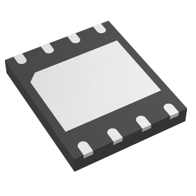
IC FLASH 512MBIT SPI/QUAD 8WSON |
|---|---|
| Quantity | 1,106 Available (as of June 14, 2026) |
| Product Category | Memory |
|---|---|
| Manufacturer | Winbond Electronics |
| Manufacturing Status | Active |
| Manufacturer Standard Lead Time | 24 Weeks |
| Datasheet |
Specifications & Environmental
| Device Package | 8-WSON (6x5) | Memory Format | FLASH | Technology | FLASH - NAND (SLC) | ||
|---|---|---|---|---|---|---|---|
| Memory Size | 512 Mbit | Access Time | 7 ns | Grade | Industrial | ||
| Clock Frequency | 166 MHz | Voltage | 2.7V ~ 3.6V | Memory Type | Non-Volatile | ||
| Operating Temperature | -40°C ~ 85°C (TA) | Write Cycle Time Word Page | 700 μs | Packaging | 8-WDFN Exposed Pad | ||
| Mounting Method | Non-Volatile | Memory Interface | SPI - Quad I/O | Memory Organization | 64M x 8 | ||
| Moisture Sensitivity Level | 3 (168 Hours) | RoHS Compliance | ROHS3 Compliant | REACH Compliance | REACH Unaffected | ||
| Qualification | N/A | ECCN | 3A991B1A | HTS Code | 8542.32.0071 |
Overview of W25N512GVPIG – IC FLASH 512Mbit SPI/QUAD 8WSON
The W25N512GVPIG is a 3.0V serial SLC NAND Flash memory device in Winbond's SpiFlash® family. It provides 512 Mbit of non-volatile storage organized as 64M × 8 and supports Dual/Quad SPI operation with buffer read and continuous read modes.
Designed for systems that require reliable serial flash storage, the device combines SLC NAND technology, a Quad I/O SPI interface and a compact 8-WSON (6×5 mm) package to address embedded code and data storage needs across a range of designs.
Key Features
- Memory Type & Capacity 512 Mbit of non-volatile SLC NAND Flash organized as 64M × 8, suitable for serial flash storage applications.
- Serial Interface SPI interface with Dual/Quad I/O support for higher I/O modes; includes buffer read and continuous read capabilities as described in the device instruction set.
- Performance Clock frequency up to 166 MHz and access time of 7 ns, enabling fast serial read operations when operated in supported modes.
- Program/Erase and Buffering Supports page program and program execute operations; includes buffer read functionality and control via configuration and status registers.
- Voltage Range Single-supply operation from 2.7 V to 3.6 V for compatibility with common 3V embedded power rails.
- Package Available in an 8-WSON (6×5 mm) / 8-WDFN exposed pad package (supplier device package: 8-WSON (6×5)).
- Operating Temperature Specified operating temperature range from –40°C to 85°C (TA) for broad environmental use.
- Reliability & Control Configuration and status registers include features such as ECC enable (ECC-E), buffer/continuous read mode (BUF) and protection bits to manage memory protection and device behavior.
- Write Performance Typical word/page write cycle time of 700 µs for program operations.
Typical Applications
- Embedded Storage Non-volatile serial storage for embedded systems requiring code or data retention in a compact SPI Flash form factor.
- Firmware / Boot Media Storage of firmware and boot code using serial SLC NAND Flash with support for Dual/Quad SPI read modes and device identification instructions.
- Consumer and Industrial Electronics General-purpose flash storage in designs that operate within the specified 2.7 V–3.6 V supply and –40°C to 85°C temperature range.
Unique Advantages
- High-density SLC NAND 512 Mbit capacity in a single 64M × 8 device provides substantial non-volatile storage without external memory stacking.
- Flexible SPI I/O Modes Dual and Quad SPI support plus buffer/continuous read modes offer flexible performance and throughput choices tied directly to the device instruction set.
- Wide Voltage Compatibility 2.7 V–3.6 V supply range enables straightforward integration into common embedded power domains.
- Compact, Thermally Friendly Package 8‑WSON (6×5 mm) with exposed pad provides a small footprint and a thermal path for board-level designs.
- Configurable Protection and ECC Status and configuration registers include protection bits, OTP lock options, and an ECC enable control to manage data integrity and memory protection.
- Industrial Temperature Range –40°C to 85°C operating range supports deployment in a broad set of environmental conditions.
Why Choose W25N512GVPIG?
The W25N512GVPIG positions itself as a high-density serial SLC NAND Flash solution for designs that need reliable non-volatile storage with flexible SPI interface options. Its combination of 512 Mbit capacity, Dual/Quad SPI support, buffer/continuous read modes and configurable protection registers makes it suitable for embedded systems and firmware storage applications where performance and control are required.
Engineers designing to a 3V power rail and operating across –40°C to 85°C will find the W25N512GVPIG offers a compact package option and register-level controls (including ECC and protection features) that help manage data integrity and device behavior across product lifecycles.
Request a quote or submit an RFQ to receive pricing and availability information for the W25N512GVPIG.