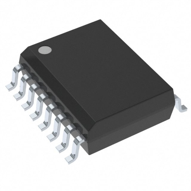
W25N512GVFIR
| Part Description |
IC FLASH 512MBIT SPI/QUAD 16SOIC |
|---|---|
| Quantity | 668 Available (as of June 15, 2026) |

| Product Category | Memory |
|---|---|
| Manufacturer | Winbond Electronics |
| Manufacturing Status | Active |
| Manufacturer Standard Lead Time | 24 Weeks |
| Datasheet |
Specifications & Environmental
| Device Package | 16-SOIC | Memory Format | FLASH | Technology | FLASH - NAND (SLC) | ||
|---|---|---|---|---|---|---|---|
| Memory Size | 512 Mbit | Access Time | 6 ns | Grade | Industrial | ||
| Clock Frequency | 166 MHz | Voltage | 2.7V ~ 3.6V | Memory Type | Non-Volatile | ||
| Operating Temperature | -40°C ~ 85°C (TA) | Write Cycle Time Word Page | 700 μs | Packaging | 16-SOIC (0.295", 7.50mm Width) | ||
| Mounting Method | Non-Volatile | Memory Interface | SPI - Quad I/O | Memory Organization | 64M x 8 | ||
| Moisture Sensitivity Level | 3 (168 Hours) | RoHS Compliance | ROHS3 Compliant | REACH Compliance | REACH Unaffected | ||
| Qualification | N/A | ECCN | 3A991B1A | HTS Code | 8542.32.0071 |
Overview of W25N512GVFIR – IC FLASH 512MBIT SPI/QUAD 16SOIC
The W25N512GVFIR is a 3V, 512 M-bit serial SLC NAND Flash memory from Winbond Electronics' SpiFlash® series. It implements Dual/Quad SPI with buffer read and continuous read modes to deliver high-density, non-volatile storage in a serial flash form factor.
Designed for systems requiring 512 Mbit of non-volatile storage with high-speed SPI/Quad I/O access, the device combines SLC NAND technology, a 64M × 8 memory organization and a 16-SOIC package to support embedded storage, firmware and data retention in compact PCB designs.
Key Features
- Memory Architecture 512 Mbit serial SLC NAND Flash organized as 64M × 8 for non-volatile data and code storage.
- Interface and Command Support Dual/Quad SPI interface (Quad I/O) with support for standard, dual and quad SPI instructions, buffer read and continuous read modes as documented in the device instruction set.
- Performance Supports up to 166 MHz clock frequency and lists an access time of 6 ns for read operations; includes support for buffer read and continuous read modes to optimize throughput.
- Program/Erase Supports program and erase operations including 128 KB block erase (D8h) and page program sequences; typical write cycle time (word/page) specified as 700 μs.
- Protection and Configuration Status and configuration registers with volatile writable and OTP-lockable bits, protection registers, ECC enable control and other register-based protection features documented in the datasheet.
- Power and Temperature Single-supply operation from 2.7 V to 3.6 V and an operating ambient temperature range of −40°C to 85°C (TA).
- Package 16-SOIC (300 mil / 0.295" width, 7.50 mm) surface-mount package suitable for compact board layouts.
Typical Applications
- Embedded systems Provides 512 Mbit of non-volatile storage for firmware, configuration data and lookup tables in board-level embedded designs.
- Code and data storage Suitable for storing code images and persistent data where serial SLC NAND density and SPI/Quad access are required.
- Consumer and industrial electronics Fits compact PCB footprints that require a 16-SOIC package combined with industrial temperature range operation (−40°C to 85°C).
Unique Advantages
- High-density SLC NAND 512 Mbit capacity organized as 64M × 8 delivers large non-volatile storage in a serial flash package.
- High-speed Quad SPI I/O Dual/Quad SPI interface and support for up to 166 MHz clock frequency enable faster serial read throughput compared with single-I/O modes.
- Flexible power range Operates from 2.7 V to 3.6 V to accommodate 3V system rails and common embedded power domains.
- Industrial temperature support Rated for −40°C to 85°C ambient, enabling deployment in a wide range of environmental conditions.
- On-chip protection and configurability Multiple status/configuration registers, OTP-lockable bits and ECC control provide firmware-level protection and configuration options as described in the datasheet.
- Compact SOIC form factor 16-SOIC package (0.295", 7.50 mm width) for space-constrained PCB designs.
Why Choose W25N512GVFIR?
The W25N512GVFIR combines a 512 Mbit SLC NAND architecture with Dual/Quad SPI and buffer/continuous read capabilities to deliver a high-density, serial flash memory solution for embedded applications. Its 166 MHz clock capability, configurable protection registers and ECC options provide designers with performance and control tied directly to the device specification.
This device is suited for designs that require large non-volatile storage in a compact 16-SOIC package and operation across a −40°C to 85°C ambient range, with a 2.7 V to 3.6 V supply window. Detailed instruction sets, protection schemes and functional descriptions are documented in the product datasheet to support integration and firmware control.
If you need pricing, lead time or a formal quote for W25N512GVFIR, request a quote or submit a product inquiry to obtain current availability and ordering information.