W25N512GVEIT TR
| Part Description |
IC FLASH 512MBIT SPI/QUAD 8WSON |
|---|---|
| Quantity | 1,244 Available (as of June 15, 2026) |

| Product Category | Memory |
|---|---|
| Manufacturer | Winbond Electronics |
| Manufacturing Status | Active |
| Manufacturer Standard Lead Time | 24 Weeks |
| Datasheet |
Specifications & Environmental
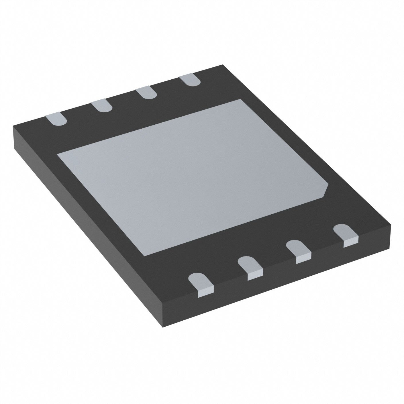
| Device Package | 8-WSON (8x6) | Memory Format | FLASH | Technology | FLASH - NAND (SLC) | ||
|---|---|---|---|---|---|---|---|
| Memory Size | 512 Mbit | Access Time | 6 ns | Grade | Industrial | ||
| Clock Frequency | 166 MHz | Voltage | 2.7V ~ 3.6V | Memory Type | Non-Volatile | ||
| Operating Temperature | -40°C ~ 85°C (TA) | Write Cycle Time Word Page | 700 μs | Packaging | 8-WDFN Exposed Pad | ||
| Mounting Method | Non-Volatile | Memory Interface | SPI - Quad I/O | Memory Organization | 64M x 8 | ||
| Moisture Sensitivity Level | 3 (168 Hours) | RoHS Compliance | ROHS3 Compliant | REACH Compliance | REACH Unaffected | ||
| Qualification | N/A | ECCN | 3A991B1A | HTS Code | 8542.32.0071 |
Overview of W25N512GVEIT TR – IC FLASH 512MBIT SPI/QUAD 8WSON
The W25N512GVEIT TR is a 512 Mbit serial SLC NAND flash memory device in a Quad SPI configuration. It provides non-volatile storage organized as 64M x 8 with Dual/Quad SPI support, buffer read and continuous read modes for flexible read performance.
Designed for embedded storage applications, the device operates from 2.7 V to 3.6 V and across a -40 °C to 85 °C ambient range, offering a combination of density, interface flexibility and documented functional control for system firmware, code shadowing and data storage.
Key Features
- Memory Core
512 Mbit SLC NAND flash organized as 64M x 8, providing non-volatile storage in a single-chip solution. - Serial Interface
Supports SPI with Dual and Quad I/O modes to maximize throughput while using standard SPI signaling. - High-Speed Operation
Clock frequency up to 166 MHz and an access time of 6 ns for fast serial read access; includes buffer read and continuous read modes as documented in the datasheet. - Program/Erase Characteristics
Page/word program and erase sequencing with a typical write cycle time for word/page operations of 700 µs. - Voltage and Temperature
Operates from 2.7 V to 3.6 V and across an ambient temperature range of -40 °C to 85 °C. - Package
Offered in an 8-WSON (8×6 mm) / 8-WDFN package with an exposed pad; package and pin configurations are described in the device documentation. - Device Control and Status
Detailed protection, configuration and status registers are defined (including volatile/OTP-lockable bits, ECC status, and busy/progress indicators) to manage memory operations and protection.
Typical Applications
- Embedded Systems
Non-volatile code and data storage for microcontroller-based systems requiring 512 Mbit of SLC NAND flash. - Firmware Storage
Storage for boot code, firmware images and system updates using serial SPI/Quad I/O interfaces. - Industrial Equipment
Data logging and storage in equipment operating across -40 °C to 85 °C where single-chip flash density and SPI connectivity are required. - Consumer Electronics
High-density external flash for feature storage and content delivery using standard SPI and higher-throughput Quad modes.
Unique Advantages
- High-density SLC storage: 512 Mbit organized as 64M x 8 provides substantial non-volatile capacity in a single device.
- Flexible high-speed SPI interface: Dual/Quad SPI support and up to 166 MHz clock frequency enable improved serial throughput compared with standard SPI-only devices.
- Detailed control and protection: Extensive status, configuration and protection registers (including OTP-lockable bits and ECC status) give precise management of program/erase and protection features.
- Wide supply and temperature range: 2.7 V–3.6 V supply and -40 °C to 85 °C operating range support a broad set of embedded and industrial environments.
- Optimized read modes: Buffer read and continuous read modes allow designers to select read behaviors that match system timing and throughput requirements.
- Compact exposed-pad package: Available in an 8-WSON (8×6 mm) / 8-WDFN exposed pad package suitable for space-constrained board layouts.
Why Choose W25N512GVEIT TR?
The W25N512GVEIT TR combines 512 Mbit of SLC NAND density with Dual/Quad SPI connectivity and documented buffer/continuous read capabilities, making it suitable for embedded designs that require sizeable non-volatile storage with configurable serial throughput. Its 2.7 V–3.6 V supply range and -40 °C to 85 °C operating range align with many industrial and consumer system requirements.
The device is accompanied by comprehensive functional descriptions, instruction sets and register definitions in the product documentation, enabling controlled memory management, protection settings and read/program workflows for firmware and data storage applications.
Request a quote or contact sales to discuss volume pricing, lead times and availability for W25N512GVEIT TR and to obtain technical support or additional documentation.