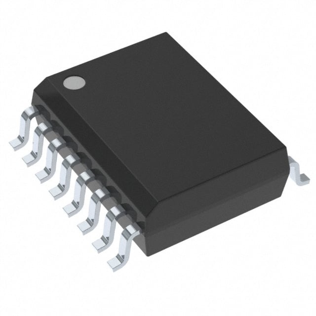
W25N512GVFIG
| Part Description |
IC FLASH 512MBIT SPI/QUAD 16SOIC |
|---|---|
| Quantity | 1,875 Available (as of June 10, 2026) |

| Product Category | Memory |
|---|---|
| Manufacturer | Winbond Electronics |
| Manufacturing Status | Active |
| Manufacturer Standard Lead Time | 24 Weeks |
| Datasheet |
Specifications & Environmental
| Device Package | 16-SOIC | Memory Format | FLASH | Technology | FLASH - NAND (SLC) | ||
|---|---|---|---|---|---|---|---|
| Memory Size | 512 Mbit | Access Time | 7 ns | Grade | Industrial | ||
| Clock Frequency | 166 MHz | Voltage | 2.7V ~ 3.6V | Memory Type | Non-Volatile | ||
| Operating Temperature | -40°C ~ 85°C (TA) | Write Cycle Time Word Page | 700 μs | Packaging | 16-SOIC (0.295", 7.50mm Width) | ||
| Mounting Method | Non-Volatile | Memory Interface | SPI - Quad I/O | Memory Organization | 64M x 8 | ||
| Moisture Sensitivity Level | 3 (168 Hours) | RoHS Compliance | ROHS3 Compliant | REACH Compliance | REACH Unaffected | ||
| Qualification | N/A | ECCN | 3A991B1A | HTS Code | 8542.32.0071 |
Overview of W25N512GVFIG – IC FLASH 512Mbit SPI/QUAD 16-SOIC
The W25N512GVFIG is a 3.0V, 512 Mbit serial SLC NAND flash memory in a 16-SOIC package. It implements serial SPI with Dual and Quad I/O modes and supports buffer read and continuous read operations as described in the device datasheet.
Designed for systems requiring non-volatile serial NAND storage, the device provides a 64M × 8 memory organization with a single-level cell (SLC) architecture, a wide supply range of 2.7V–3.6V, and an industrial operating temperature range of −40°C to 85°C.
Key Features
- Memory Architecture 512 Mbit SLC NAND flash organized as 64M × 8 for non-volatile data and code storage.
- Serial Interface SPI serial interface with Dual and Quad I/O support for higher throughput and flexible bus configurations.
- High-Speed Read Modes Buffer read and continuous read modes are supported; device clock frequency up to 166 MHz to enable faster serial transfers.
- On-Device Protection & Configuration Protection, configuration and status registers are provided, including block protect bits, write-protect enable, one-time-program (OTP) lock bits and status registers for device management.
- ECC and Status Reporting Status register bits include ECC indicators and program/erase failure flags to support error detection and system diagnostics.
- Timing and Program/Erase Typical access time listed at 7 ns and a write cycle time (word/page) of 700 µs for program operations (per datasheet specifications).
- Power Single-supply operation from 2.7V to 3.6V suitable for common 3V system rails.
- Package and Temperature Available in a 16-SOIC (300 mil, 7.50 mm width) package with an operating temperature range of −40°C to 85°C.
Typical Applications
- Embedded Storage Non-volatile storage of firmware, code images, and data where serial SLC NAND is required.
- Consumer Electronics Serial flash memory for devices that use SPI/Quad I/O interfaces and require buffer/continuous read modes.
- Industrial Systems Storage for industrial controllers and instrumentation operating across −40°C to 85°C with 3V system rails.
- Firmware and Boot Storage Reliable program and boot image storage leveraging SLC NAND organization and on-device protection registers.
Unique Advantages
- High-density SLC NAND: 512 Mbit capacity in a single device supports larger code and data storage footprints without multiple components.
- Flexible high-throughput interface: Dual/Quad SPI support and up to 166 MHz clocking enable faster serial data transfer for read-intensive operations.
- Device-level protection and configuration: Multiple protection and configuration registers, including OTP-lockable bits, provide control over block protection and status settings.
- Error visibility and management: ECC status bits and program/erase failure indicators in status registers aid diagnostics and system reliability monitoring.
- Broad operating voltage and temperature: 2.7V–3.6V supply range and −40°C to 85°C rating support a variety of 3V system designs and temperature environments.
- Compact industry-standard package: 16-SOIC package offers a standard form factor for PCB designs requiring throughflow assembly or space-constrained layouts.
Why Choose W25N512GVFIG?
The W25N512GVFIG positions itself as a 3V serial SLC NAND flash solution combining 512 Mbit density, Dual/Quad SPI connectivity and on-device protection/configuration features. Its documented buffer read and continuous read modes, ECC/status reporting, and support for higher clock rates make it suitable for embedded designs that need managed non-volatile storage and diagnostic visibility.
This device is appropriate for designers targeting systems with 3V rails and industrial temperature requirements, offering a compact 16-SOIC footprint and the control registers needed for block protection and operational configuration.
Request a quote or submit an inquiry for availability and pricing to include the W25N512GVFIG in your next design.