W25N512GVEIT
| Part Description |
IC FLASH 512MBIT SPI/QUAD 8WSON |
|---|---|
| Quantity | 928 Available (as of June 15, 2026) |

| Product Category | Memory |
|---|---|
| Manufacturer | Winbond Electronics |
| Manufacturing Status | Active |
| Manufacturer Standard Lead Time | 24 Weeks |
| Datasheet |
Specifications & Environmental
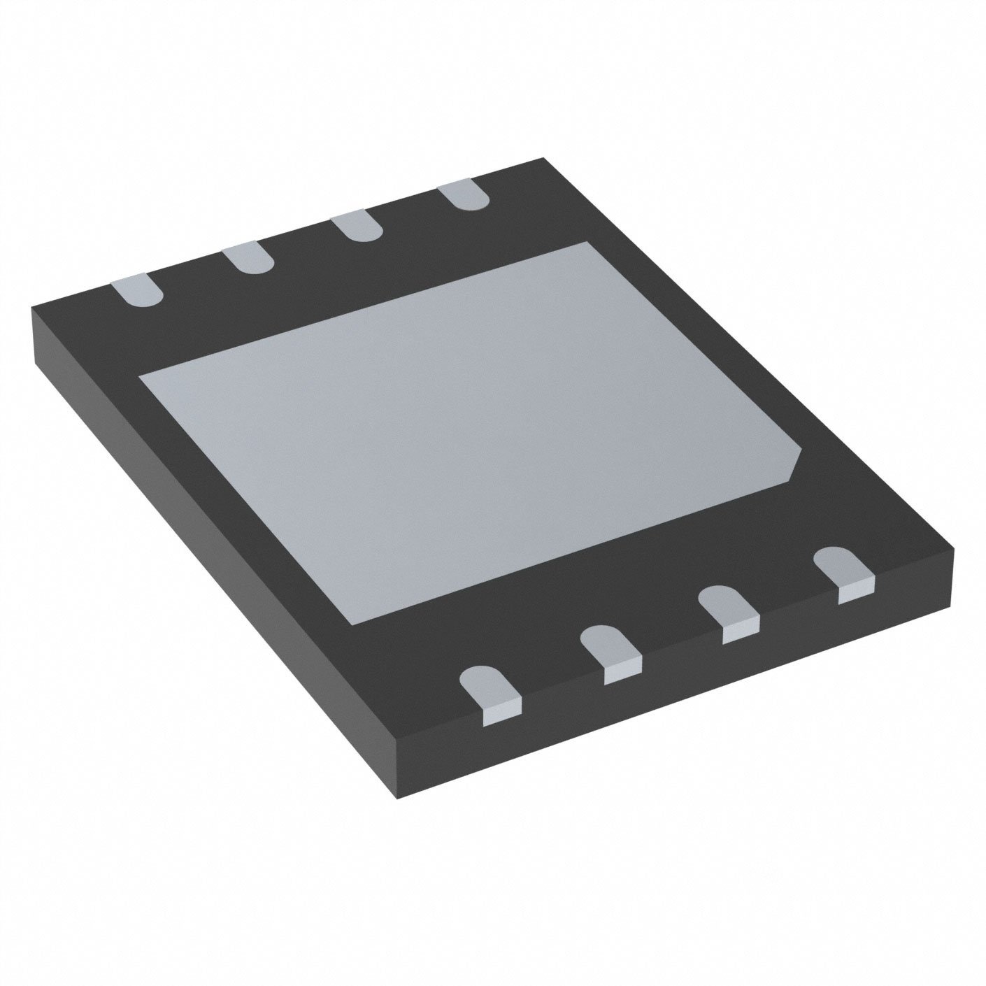
| Device Package | 8-WSON (8x6) | Memory Format | FLASH | Technology | FLASH - NAND (SLC) | ||
|---|---|---|---|---|---|---|---|
| Memory Size | 512 Mbit | Access Time | 7 ns | Grade | Industrial | ||
| Clock Frequency | 166 MHz | Voltage | 2.7V ~ 3.6V | Memory Type | Non-Volatile | ||
| Operating Temperature | -40°C ~ 85°C (TA) | Write Cycle Time Word Page | 700 μs | Packaging | 8-WDFN Exposed Pad | ||
| Mounting Method | Non-Volatile | Memory Interface | SPI - Quad I/O | Memory Organization | 64M x 8 | ||
| Moisture Sensitivity Level | 3 (168 Hours) | RoHS Compliance | ROHS3 Compliant | REACH Compliance | REACH Unaffected | ||
| Qualification | N/A | ECCN | 3A991B1A | HTS Code | 8542.32.0071 |
Overview of W25N512GVEIT – IC FLASH 512MBIT SPI/QUAD 8WSON
The W25N512GVEIT is a 512 Mbit serial SLC NAND flash memory device implementing Dual/Quad SPI I/O and designed for non-volatile data storage. It integrates buffer read and continuous read modes and provides a serial interface optimized for high-throughput read operations.
This device targets systems that require compact, high-density non-volatile memory with industry-standard SPI/Quad I/O connectivity and configurable protection and status features for robust data management.
Key Features
- Memory Type & Capacity 512 Mbit SLC NAND flash organized as 64M × 8 for byte-oriented access and efficient storage management.
- Serial Interface Supports SPI with Dual and Quad I/O modes, enabling wider data paths for accelerated read throughput.
- Read Modes Buffer Read and Continuous Read modes are supported to optimize sequential read performance and reduce host overhead.
- Performance Up to 166 MHz clock frequency and a 7 ns access time specification for responsive data access in serial operations.
- Program/Erase Timing Page program write cycle time specified at 700 µs for predictable write timing.
- Supply Voltage Operates across a 2.7 V to 3.6 V supply range to match common 3.3 V system rails.
- Package Available in an 8-WDFN exposed pad variant and listed supplier device package 8-WSON (8×6) for compact PCB mounting.
- Temperature Range Rated for operation from –40 °C to 85 °C (TA) for industrial-temperature applications.
- Protection & Management On-chip protection and configuration registers, status registers, ECC enable/monitoring bits, and bad-block management features as documented in the device instruction set and status register descriptions.
Unique Advantages
- High-density serial storage: 512 Mbit capacity in a compact serial-NAND form factor provides substantial non-volatile storage while minimizing PCB area.
- Flexible high-speed I/O: Dual/Quad SPI modes and up to 166 MHz clock support allow designers to scale read bandwidth without changing the fundamental SPI-based interface.
- Optimized sequential reads: Buffer Read and Continuous Read modes reduce host transaction overhead for large or streaming data reads.
- Predictable write timing: Specified write cycle time (700 µs) gives deterministic program timing for system-level scheduling.
- Robust data management: Built-in status, protection registers, ECC enable bits and bad-block management enable controlled protection and monitoring of stored data as described in the device documentation.
- Wide operating conditions: Operation from 2.7 V to 3.6 V and –40 °C to 85 °C supports deployment across common industrial environments and 3.3 V system designs.
Why Choose W25N512GVEIT?
The W25N512GVEIT combines SLC NAND storage density with a serial Dual/Quad SPI interface and read-optimized modes to deliver compact, high-capacity non-volatile memory for embedded systems. Its on-chip protection and status registers, ECC-related configuration bits, and bad-block management capabilities provide explicit mechanisms for data integrity and device control as described in the device documentation.
This device suits designs that require a balance of storage capacity, serial interface flexibility, and predictable timing across a 2.7 V–3.6 V power domain and –40 °C to 85 °C operating window. The exposed-pad WDFN/8-WSON package options allow compact PCB layouts while retaining the device’s functional feature set.
Request a quote or submit an inquiry to receive pricing, lead-time, and availability information for the W25N512GVEIT.