W25N512GWBIR
| Part Description |
IC FLASH 512MBIT SPI 24TFBGA |
|---|---|
| Quantity | 1,853 Available (as of June 15, 2026) |

| Product Category | Memory |
|---|---|
| Manufacturer | Winbond Electronics |
| Manufacturing Status | Active |
| Manufacturer Standard Lead Time | 28 Weeks |
| Datasheet |
Specifications & Environmental
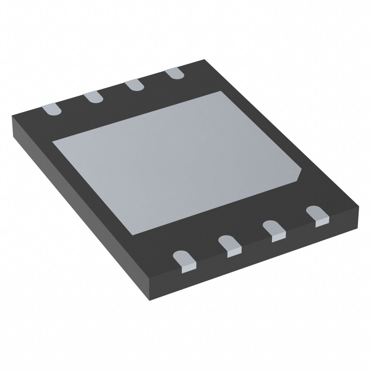
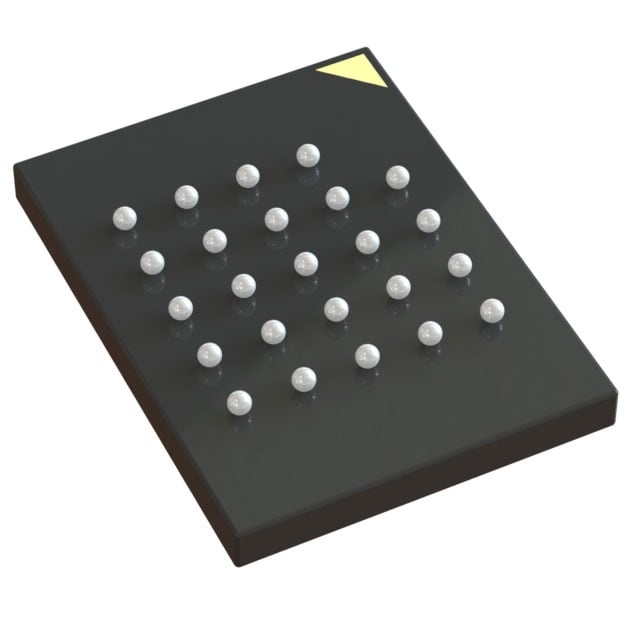
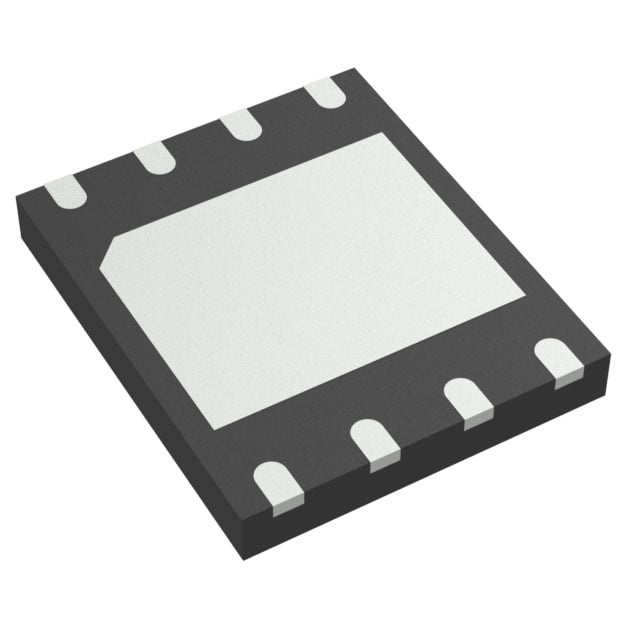
| Device Package | 24-TFBGA (6x8) | Memory Format | FLASH | Technology | FLASH - NAND (SLC) | ||
|---|---|---|---|---|---|---|---|
| Memory Size | 512 Mbit | Access Time | 7 ns | Grade | Industrial | ||
| Clock Frequency | 104 MHz | Voltage | 1.7V ~ 1.95V | Memory Type | Non-Volatile | ||
| Operating Temperature | -40°C ~ 85°C (TA) | Write Cycle Time Word Page | 700 μs | Packaging | 24-TBGA | ||
| Mounting Method | Non-Volatile | Memory Interface | SPI - Quad I/O | Memory Organization | 64M x 8 | ||
| Moisture Sensitivity Level | 3 (168 Hours) | RoHS Compliance | ROHS3 Compliant | REACH Compliance | REACH Unaffected | ||
| Qualification | N/A | ECCN | 3A991B1A | HTS Code | 8542.32.0071 |
Overview of W25N512GWBIR – 1.8V Serial SLC NAND Flash, 512 Mbit, Dual/Quad SPI
The W25N512GWBIR is a 512‑Mbit non‑volatile serial SLC NAND flash memory device implemented with Dual/Quad SPI and buffer/continuous read modes. It operates from a 1.7 V to 1.95 V supply and provides a 64M × 8 memory organization for compact, high‑density serial storage.
This device targets designs that require reliable serial flash storage with high density and flexible SPI interfaces. Key technical advantages include SLC NAND technology, hardware control and status registers for protection and ECC management, and a compact 24‑TFBGA (6×8) package for board space‑constrained applications.
Key Features
- Memory Type & Technology – 512 Mbit SLC NAND flash organized as 64M × 8, providing non‑volatile storage optimized for serial flash applications.
- Serial Interface – Supports SPI with Dual and Quad I/O modes for higher throughput in compatible host controllers.
- Performance – Clock frequency up to 104 MHz and an access time of 7 ns for read operations; buffer read and continuous read modes available in device instruction set.
- Voltage Range – Operates from 1.7 V to 1.95 V, suitable for low‑voltage system domains that require 1.8 V flash operation.
- Program/Erase Metrics – Page/program related timing includes word/page write cycle times on the order of 700 µs as specified for program operations.
- Protection & Configuration – On‑die protection and configuration features include volatile and OTP‑lockable protection bits, write protect enable, ECC enable, buffer/continuous read mode control, and multiple status registers for operation monitoring.
- Package & Mounting – Available in a compact 24‑TFBGA (6×8 mm, 5×5 ball array) package optimized for surface‑mount assembly.
- Operating Temperature – Rated for ambient operation from −40 °C to 85 °C (TA).
Typical Applications
- Firmware and Boot Storage – Non‑volatile storage for system firmware, boot code, and configuration data where serial flash is required.
- Code and Data Storage – External serial memory for storing lookup tables, calibration data, and application code with controlled protection and ECC options.
- Embedded Systems – Compact flash storage in board designs requiring a 24‑TFBGA package and 1.8 V operation.
Unique Advantages
- High‑Density SLC NAND: 512 Mbit SLC architecture provides a dense non‑volatile storage option while maintaining SLC characteristics described in the device documentation.
- Flexible SPI Throughput: Dual and Quad SPI support plus a 104 MHz clock rating enable higher data rates where the host interface supports multi‑I/O SPI modes.
- On‑Die Protection Controls: Volatile and OTP‑lockable protection bits, write protect enable and status registers allow controlled data and region protection as documented.
- Buffer and Continuous Read Modes: Configurable buffer read and continuous read modes help tailor read behavior to system requirements as specified in the instruction set.
- Compact Surface‑Mount Package: 24‑TFBGA (6×8 mm) package minimizes board area for space‑constrained designs.
- Wide Ambient Range: −40 °C to 85 °C rating supports a broad set of commercial and industrial ambient conditions.
Why Choose IC FLASH 512MBIT SPI 24TFBGA?
The W25N512GWBIR positions itself as a compact, high‑density serial SLC NAND flash solution combining Dual/Quad SPI interfaces, configurable buffer/continuous read modes, and on‑die protection and status registers. Its 1.7 V–1.95 V supply range, 104 MHz clock capability, and 24‑TFBGA package make it suitable for designs that require dense non‑volatile serial storage with configurable protection and ECC control.
This device is a fit for engineers seeking a documented SLC NAND flash with explicit programming, protection and status features, and a compact package for constrained board layouts. The combination of memory density, interface flexibility and documented control registers supports long‑term integration into embedded storage designs.
If you require pricing, availability, or a formal quote for W25N512GWBIR, please request a quote or contact sales to submit a quotation request and obtain further procurement details.