W9825G6JH-6I TR
| Part Description |
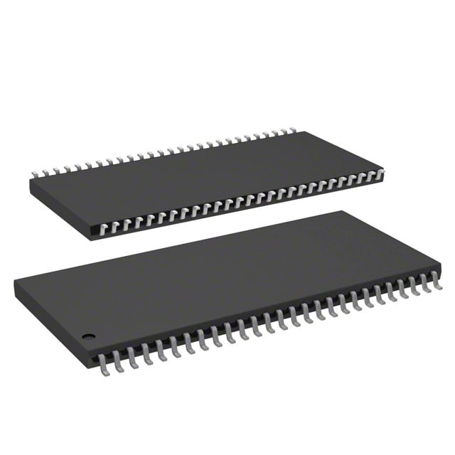
IC DRAM 256MBIT PAR 54TSOP II |
|---|---|
| Quantity | 1,105 Available (as of June 15, 2026) |
| Product Category | Memory |
|---|---|
| Manufacturer | Winbond Electronics |
| Manufacturing Status | Obsolete |
| Manufacturer Standard Lead Time | Contact Us |
| Datasheet |
Specifications & Environmental
| Device Package | 54-TSOP II | Memory Format | DRAM | Technology | SDRAM | ||
|---|---|---|---|---|---|---|---|
| Memory Size | 256 Mbit | Access Time | 5 ns | Grade | Industrial | ||
| Clock Frequency | 166 MHz | Voltage | 3V ~ 3.6V | Memory Type | Volatile | ||
| Operating Temperature | -40°C ~ 85°C (TA) | Write Cycle Time Word Page | N/A | Packaging | 54-TSOP (0.400", 10.16mm Width) | ||
| Mounting Method | Volatile | Memory Interface | Parallel | Memory Organization | 16M x 16 | ||
| Moisture Sensitivity Level | 3 (168 Hours) | RoHS Compliance | ROHS3 Compliant | REACH Compliance | REACH Unaffected | ||
| Qualification | N/A | ECCN | EAR99 | HTS Code | 8542.32.0024 |
Overview of W9825G6JH-6I TR – IC DRAM 256Mbit Parallel SDRAM, 54‑TSOP II
The W9825G6JH-6I TR is a 256 Mbit synchronous DRAM (SDRAM) organized for parallel memory systems. It implements a banked architecture (documented as 4M × 4 banks × 16 bits and listed as 16M × 16) and is offered in the 54‑lead TSOP II (0.400", 10.16 mm width) package.
This device targets applications that require parallel SDRAM memory with documented timing, standard SDRAM command support and operation at 166 MHz for the -6I speed grade. Key value is provided through its banked architecture and standard SDRAM feature set for system memory use cases that depend on predictable timing and established command sequences.
Key Features
- Memory Architecture 256 Mbit SDRAM organized as 4M × 4 banks × 16 bits (also listed as 16M × 16), enabling banked read/write sequences and burst operations as described in the device documentation.
- Speed Grades & Clock -6I speed grade compliant to 166 MHz/CL3; the datasheet documents multiple speed grades including -5, -6, -6I and -75 for different frequency/latency combinations.
- Performance Timing Typical access time indicated as 5 ns; comprehensive AC timing tables, waveforms and operating timing examples are provided in the datasheet for system integration.
- Standard SDRAM Command Set Supports mode register set, bank activate, burst read/write, auto-precharge, precharge, auto-refresh, self-refresh and power-down commands as documented (see functional description and command timing sections).
- Voltage Range Operates from 3.0 V to 3.6 V, enabling use with 3.3 V system rails.
- Package 54‑lead TSOP II (0.400", 10.16 mm width) package; package specification and mechanical drawings are included in the datasheet.
- Operating Temperature Specified ambient operating range of -40 °C to 85 °C (TA).
- Documentation Detailed functional descriptions, timing diagrams and operating examples (including bank interleaving and burst examples) are provided in the device documentation to support design and validation.
Typical Applications
- Computing platforms System memory for computing and PC-class designs where parallel SDRAM and defined timing behavior are required.
- Embedded systems General-purpose parallel memory for embedded controllers and boards that require mid-density SDRAM with banked access.
- Industrial equipment Memory modules in systems operating across a wide ambient temperature range (−40 °C to 85 °C).
Unique Advantages
- Banked SDRAM Architecture: 4-bank organization provides flexible burst and interleaved access patterns to improve throughput for sequential and interleaved workloads.
- Documented Timing and Examples: Extensive timing tables, waveforms and operating examples simplify integration and reduce design iteration.
- Standard Command Support: Full SDRAM command set (mode register, auto-refresh, self-refresh, power-down, burst operations) supports established memory control schemes.
- Wide Supply Window: 3.0–3.6 V operating range aligns with common 3.3 V systems for straightforward power design.
- Broad Temperature Range: Specified operation from −40 °C to 85 °C for use in temperature-varied environments.
- Industry‑standard Package: 54‑lead TSOP II (400 mil) package with package specification provided for board-level mechanical design.
Why Choose W9825G6JH-6I TR?
The W9825G6JH-6I TR provides a documented, banked SDRAM option in a compact 54‑TSOP II package for designs that require a mid-density (256 Mbit) parallel SDRAM with defined timing and command behavior. Its 166 MHz -6I grading and included timing resources make it appropriate for systems that need predictable burst and interleaved access patterns, while the 3.0–3.6 V supply range and −40 °C to 85 °C operating window support deployment across a range of environments.
Choose this part when you need an SDRAM device with full SDRAM command support, comprehensive datasheet timing and package documentation to accelerate system integration and validation.
Request a quote or submit a sales inquiry for pricing, availability and lead-time information.