W9825G6KB-6
| Part Description |
IC DRAM 256MBIT PAR 54TFBGA |
|---|---|
| Quantity | 642 Available (as of June 15, 2026) |
| Product Category | Memory |
|---|---|
| Manufacturer | Winbond Electronics |
| Manufacturing Status | Active |
| Manufacturer Standard Lead Time | 24 Weeks |
| Datasheet |
Specifications & Environmental
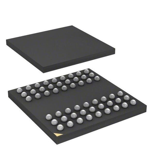
| Device Package | 54-TFBGA (8x8) | Memory Format | DRAM | Technology | SDRAM | ||
|---|---|---|---|---|---|---|---|
| Memory Size | 256 Mbit | Access Time | 5 ns | Grade | Commercial | ||
| Clock Frequency | 133 MHz | Voltage | 3V ~ 3.6V | Memory Type | Volatile | ||
| Operating Temperature | 0°C ~ 70°C (TC) | Write Cycle Time Word Page | N/A | Packaging | 54-TFBGA | ||
| Mounting Method | Volatile | Memory Interface | Parallel | Memory Organization | 16M x 16 | ||
| Moisture Sensitivity Level | 3 (168 Hours) | RoHS Compliance | ROHS3 Compliant | REACH Compliance | REACH Unaffected | ||
| Qualification | N/A | ECCN | EAR99 | HTS Code | 8542.32.0024 |
Overview of W9825G6KB-6 – IC DRAM 256MBIT PAR 54TFBGA
The W9825G6KB-6 is a high-speed synchronous DRAM (SDRAM) device from Winbond Electronics, organized for parallel memory systems with a 16-bit data path and a total density of 256 Mbit. The device implements a banked memory architecture and standard SDRAM control functions to support burst read/write operations and memory management features such as auto-precharge and self-refresh.
Key electrical and mechanical attributes include a 3.0–3.6 V supply range, a 54‑TFBGA (8×8) package, and an operating case temperature range of 0°C to 70°C. The device is provided in the -6 speed grade and the datasheet documents banked operation and timing for high-throughput memory applications.
Key Features
- Memory architecture Organized as 4M × 4 banks × 16 bits (equivalent to a 16M × 16 organization) delivering 256 Mbit total capacity.
- SDRAM core Synchronous DRAM with a parallel memory interface and standard SDRAM command set for predictable, burst-oriented data transfers.
- Performance Specified with a clock frequency of 133 MHz and an access time of 5 ns; the datasheet also references delivered bandwidth capability in its operating description.
- Advanced memory controls Supports bank activate, burst read/write, burst stop, auto-precharge, precharge, self-refresh and power-down modes as documented in the datasheet command set and timing sections.
- Operating voltage Designed for 3.0 V to 3.6 V supply rails.
- Package and mounting 54‑TFBGA (8×8) package for board-level BGA mounting and high-density integration.
- Thermal range Rated for an operating case temperature (TC) range of 0°C to 70°C.
Typical Applications
- Personal computer memory subsystems Documented in the datasheet as aligned to PC industrial speed grades, suitable where a 256 Mbit SDRAM device is required in parallel memory architectures.
- Board-level DRAM modules Use on OEM PCBs requiring a compact 54‑TFBGA 256 Mbit SDRAM package for on-board system memory.
- Computing systems with parallel memory interface Systems requiring a 16-bit parallel SDRAM interface and banked memory control for burst transfers and self-refresh capability.
Unique Advantages
- Compact BGA footprint: The 54‑TFBGA (8×8) package enables high-density board integration and a small PCB area for the memory component.
- Banked memory organization: 4 banks × 16-bit organization allows interleaved and burst operations for efficient access patterns as detailed in the device functional description.
- Predictable parallel interface: Parallel SDRAM interface with documented timing and command sets supports deterministic memory control and integration into parallel bus systems.
- High-speed timing: 133 MHz clock specification and 5 ns access time enable fast read/write cycles for throughput-sensitive designs.
- Standard SDRAM features: Built-in support for auto-precharge, self-refresh, power-down and other SDRAM commands simplifies memory management in system firmware.
- Established manufacturer and documentation: Winbond Electronics product with a published datasheet covering functional description, timing, and package specification.
Why Choose IC DRAM 256MBIT PAR 54TFBGA?
The W9825G6KB-6 offers an established SDRAM architecture in a compact 54‑TFBGA package, combining a 16-bit data path and a banked memory structure to support burst transfers and standard SDRAM control sequences. Its electrical specifications—3.0–3.6 V supply, 133 MHz clock rating, and 5 ns access time—make it appropriate for designs that require documented timing and predictable parallel-memory behavior.
Choose this Winbond SDRAM when your design requires a 256 Mbit parallel DRAM device with on-die support for self-refresh, power-down, and auto-precharge, and when a compact BGA footprint and manufacturer datasheet-level detail are important for system integration and validation.
If you need pricing or lead-time information, request a quote or submit a pricing inquiry referencing the W9825G6KB-6 part number and your quantity requirements.