W9825G6KB-6 TR
| Part Description |
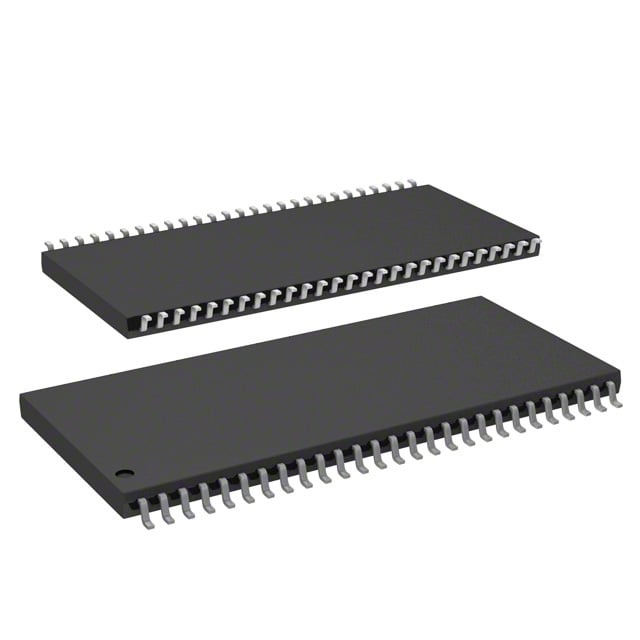
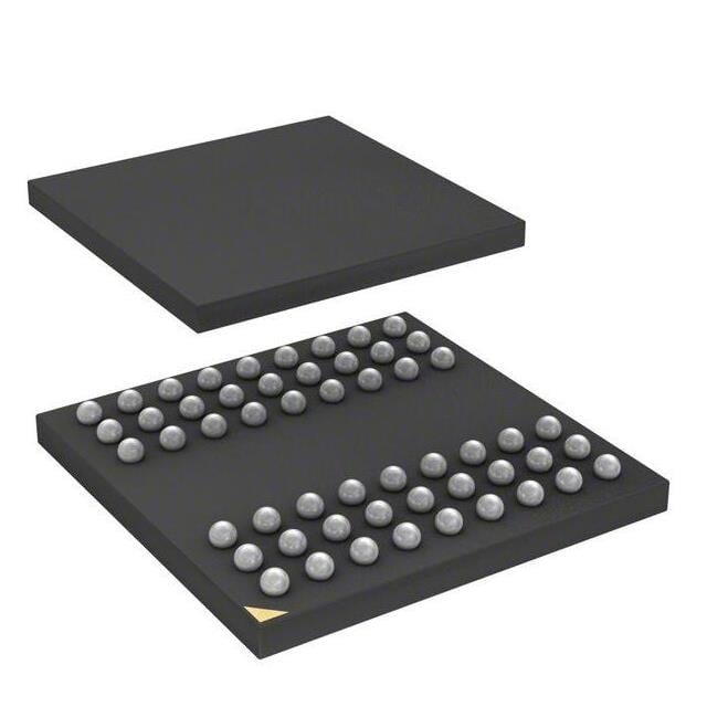
IC DRAM 256MBIT LVTTL 54TFBGA |
|---|---|
| Quantity | 585 Available (as of June 15, 2026) |

| Product Category | DRAM Memory |
|---|---|
| Manufacturer | Winbond Electronics |
| Manufacturing Status | Active |
| Manufacturer Standard Lead Time | 24 Weeks |
| Datasheet |
Specifications & Environmental
| Device Package | 54-TFBGA (8x8) | Memory Format | DRAM | Technology | SDRAM | ||
|---|---|---|---|---|---|---|---|
| Memory Size | 256 Mbit | Access Time | 5 ns | Grade | Commercial | ||
| Clock Frequency | 166 MHz | Voltage | 3V ~ 3.6V | Memory Type | Volatile | ||
| Operating Temperature | 0°C ~ 70°C (TC) | Write Cycle Time Word Page | N/A | Packaging | 54-TFBGA | ||
| Mounting Method | Volatile | Memory Interface | LVTTL | Memory Organization | 16M x 16 | ||
| Moisture Sensitivity Level | 3 (168 Hours) | RoHS Compliance | ROHS3 Compliant | REACH Compliance | REACH Unaffected | ||
| Qualification | N/A | ECCN | EAR99 | HTS Code | 8542.32.0024 |
Overview of W9825G6KB-6 TR – IC DRAM 256MBIT LVTTL 54TFBGA
The W9825G6KB-6 TR from Winbond Electronics is a high‑speed synchronous dynamic RAM (SDRAM) device organized as 16M × 16 (4M × 4 banks × 16 bits) delivering a 256 Mbit memory capacity. It implements standard SDRAM functionality including burst read/write, auto‑precharge, power‑down and self‑refresh modes and is specified for a 166 MHz clock frequency with a 5 ns access time.
Designed for systems that require a 3.0–3.6 V LVTTL memory interface in a compact 54‑TFBGA (8×8) package, this device targets applications needing synchronous DRAM storage with defined operating conditions (0 °C to 70 °C case temperature).
Key Features
- SDRAM Core Organized as 4M × 4 banks × 16 bits (16M × 16) to provide 256 Mbit of volatile memory in a standard SDRAM architecture.
- Clock and Performance Rated for a 166 MHz clock frequency with a 5 ns access time; datasheet examples and timing charts include CAS‑latency and burst operation modes.
- Standard SDRAM Function Set Supports burst read/write, auto‑precharge, precharge, self‑refresh, power‑down and command types defined in the device functional description.
- Interface LVTTL memory interface for command, address and data signaling consistent with the device functional and timing specifications.
- Power Operating supply range of 3.0 V to 3.6 V with power management modes (power‑down and self‑refresh) documented in the datasheet.
- Package 54‑TFBGA (8×8) ball grid array package for compact mounting and board‑level integration.
- Operating Temperature Specified case temperature range of 0 °C to 70 °C (TC).
Typical Applications
- Synchronous DRAM storage — Where a 256 Mbit SDRAM with 166 MHz clocking and LVTTL interface is required for high‑speed volatile data storage.
- Burst data buffering — Use in systems that leverage burst read/write and auto‑precharge features for sequential or interleaved access patterns.
- Compact board designs — Suited to designs needing a small 54‑TFBGA (8×8) package footprint with standard SDRAM timing and control.
Unique Advantages
- Verified SDRAM architecture — Detailed functional description and timing diagrams (including burst and CAS timing) provide clear integration guidance.
- Measured access performance — 5 ns access time and 166 MHz-rated operation support timely data transfers for synchronous memory subsystems.
- Standard LVTTL signaling — Simplifies interface design where LVTTL-compatible command and data signaling is required.
- Power management modes — Built‑in power‑down and self‑refresh commands reduce active power when full operation is not required.
- Compact BGA package — 54‑TFBGA (8×8) format enables space‑efficient placement on populated PCBs.
- Wide supply margin — 3.0 V to 3.6 V supply range accommodates systems with nominal 3.3 V rails.
Why Choose W9825G6KB-6 TR?
The W9825G6KB-6 TR provides a documented SDRAM solution with explicit timing, command and power‑management behavior suitable for designs requiring 256 Mbit of synchronous volatile memory. Its 166 MHz rating, 5 ns access time, LVTTL interface and compact 54‑TFBGA package make it appropriate for board designs that demand standardized SDRAM feature sets and measured timing characteristics.
Choose this device for projects where clear datasheet guidance on burst operation, command sequences (including auto‑precharge and self‑refresh) and package footprint are important for reliable integration and predictable memory behavior.
If you would like pricing, lead times or a formal quote for W9825G6KB-6 TR, please request a quote or submit an RFQ with your quantity and required delivery details.