W9825G6JB-6I
| Part Description |
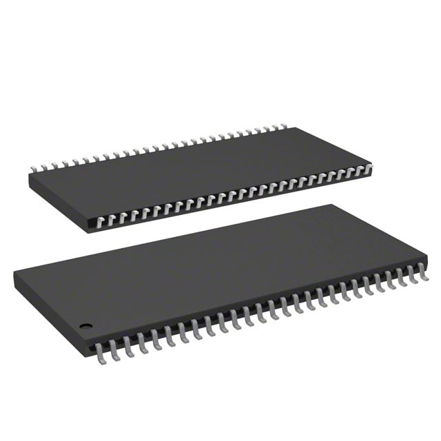
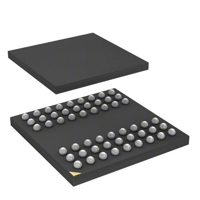
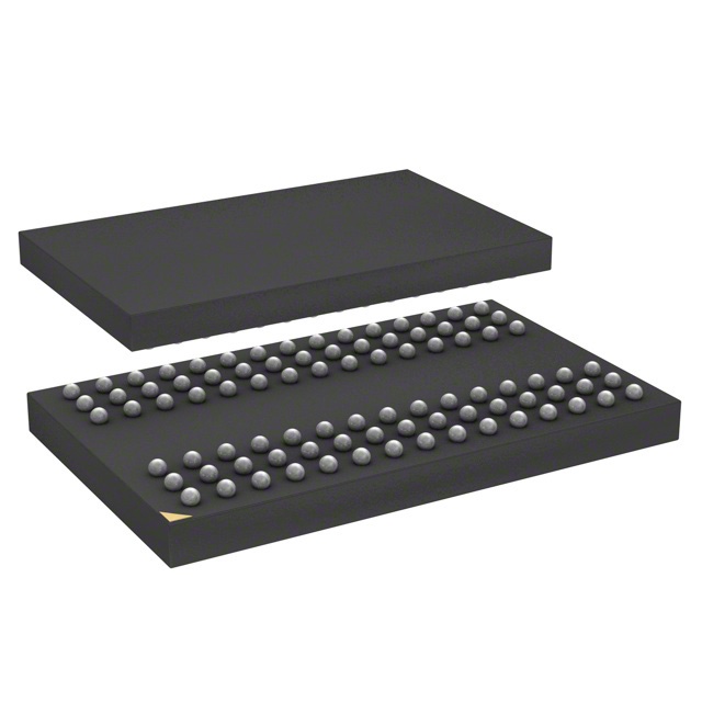
IC DRAM 256MBIT LVTTL 54TFBGA |
|---|---|
| Quantity | 1,015 Available (as of June 10, 2026) |

| Product Category | Memory |
|---|---|
| Manufacturer | Winbond Electronics |
| Manufacturing Status | Active |
| Manufacturer Standard Lead Time | 24 Weeks |
| Datasheet |
Specifications & Environmental
| Device Package | 54-TFBGA (8x8) | Memory Format | DRAM | Technology | SDRAM | ||
|---|---|---|---|---|---|---|---|
| Memory Size | 256 Mbit | Access Time | 5 ns | Grade | Industrial | ||
| Clock Frequency | 166 MHz | Voltage | 3V ~ 3.6V | Memory Type | Volatile | ||
| Operating Temperature | -40°C ~ 85°C (TA) | Write Cycle Time Word Page | N/A | Packaging | 54-TFBGA | ||
| Mounting Method | Volatile | Memory Interface | LVTTL | Memory Organization | 16M x 16 | ||
| Moisture Sensitivity Level | 3 (168 Hours) | RoHS Compliance | ROHS3 Compliant | REACH Compliance | REACH Unaffected | ||
| Qualification | N/A | ECCN | EAR99 | HTS Code | 8542.32.0024 |
Overview of W9825G6JB-6I – IC DRAM 256Mbit LVTTL 54TFBGA
The W9825G6JB-6I is a high-speed synchronous dynamic random access memory (SDRAM) device offering 256 Mbit density organized as 16M × 16. It implements a multi-bank architecture and burst-oriented access to deliver up to 166 MHz operation and a reported data bandwidth of up to 166M words per second.
Designed with an LVTTL memory interface and a 54‑TFBGA (8×8) package, the device targets systems that require synchronous DRAM with 3.0–3.6 V supply range, a 5 ns access time, and operation across an industrial temperature window of -40°C to 85°C.
Key Features
- Core / Memory 256 Mbit SDRAM organized as 16M × 16 with internal organization described as 4M × 4 banks × 16 bits for banked access.
- Performance Supports up to 166 MHz clock frequency and delivers a data bandwidth up to 166M words per second; access time specified at 5 ns.
- Interface LVTTL memory interface for synchronous control and data transfer.
- Power Operates from a 3.0 V to 3.6 V supply range as specified in the product data.
- Operational Modes & Control Burst-oriented access with support for burst read/write, mode register set, auto-precharge, self-refresh, power-down and no-op/deselect commands as described in the device functional description.
- Package & Mounting 54‑TFBGA package (8×8) for compact surface-mount implementation.
- Temperature Range Guaranteed operation across -40°C to 85°C (TA) for the -6I grade.
Typical Applications
- Embedded systems Use as system SDRAM where synchronous burst transfers, a 166 MHz clock domain and industrial temperature operation are required.
- Industrial control Suitable for control and data buffering tasks that need 256 Mbit density and operation from 3.0–3.6 V across -40°C to 85°C.
- High-speed buffering For applications needing burst-oriented read/write and multi-bank access to sustain data throughput in time-critical interfaces.
Unique Advantages
- High throughput at 166 MHz: Enables sustained data transfers up to the device's specified 166M words per second.
- Banked architecture: Internal organization of 4 banks × 16 bits supports interleaved access and improved effective throughput for burst operations.
- Burst and power-management features: Built-in support for burst read/write, auto-precharge, self-refresh and power-down modes provides flexible performance vs. power trade-offs.
- Industrial temperature support: The -6I grade is specified for -40°C to 85°C, matching designs that require an extended operating range.
- Compact BGA footprint: 54‑TFBGA (8×8) package minimizes PCB area while retaining full SDRAM functionality.
- <strong_Wide supply tolerance: Operation across a 3.0–3.6 V range simplifies integration into 3.3 V system power domains.
Why Choose W9825G6JB-6I?
The W9825G6JB-6I combines a 256 Mbit SDRAM architecture with LVTTL interfacing, a compact 54‑TFBGA package and an industrial operating temperature range to serve designs that need synchronous, burst-oriented memory with predictable timing. Its multi-bank organization and support for standard SDRAM commands and power-management modes provide flexible performance scaling and system-level control.
This device is suited to engineers and procurement teams specifying board-level SDRAM where 166 MHz operation, 5 ns access timing, and a 3.0–3.6 V supply are required. The datasheet-backed feature set supports detailed timing, mode, and power configurations for integration into time-sensitive and temperature-challenged designs.
If you need pricing, lead-time information or a formal quote for W9825G6JB-6I, please request a quote or submit an inquiry with your quantity and delivery requirements.