W9864G6KT-6
| Part Description |
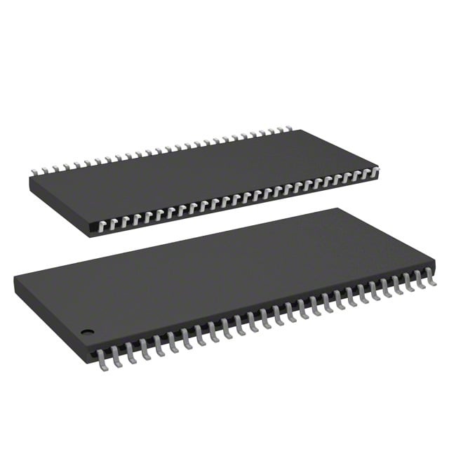
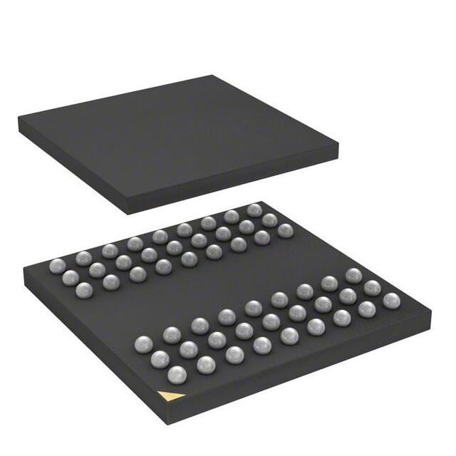
IC DRAM 64MBIT LVTTL 54TFBGA |
|---|---|
| Quantity | 910 Available (as of June 13, 2026) |

| Product Category | Memory |
|---|---|
| Manufacturer | Winbond Electronics |
| Manufacturing Status | Active |
| Manufacturer Standard Lead Time | 24 Weeks |
| Datasheet |
Specifications & Environmental
| Device Package | 54-TFBGA (8x8) | Memory Format | DRAM | Technology | SDRAM | ||
|---|---|---|---|---|---|---|---|
| Memory Size | 64 Mbit | Access Time | 5 ns | Grade | Commercial | ||
| Clock Frequency | 166 MHz | Voltage | 3V ~ 3.6V | Memory Type | Volatile | ||
| Operating Temperature | 0°C ~ 70°C (TA) | Write Cycle Time Word Page | N/A | Packaging | 54-VFBGA | ||
| Mounting Method | Volatile | Memory Interface | LVTTL | Memory Organization | 4M x 16 | ||
| Moisture Sensitivity Level | 3 (168 Hours) | RoHS Compliance | ROHS3 Compliant | REACH Compliance | REACH Unaffected | ||
| Qualification | N/A | ECCN | EAR99 | HTS Code | 8542.32.0002 |
Overview of W9864G6KT-6 – IC DRAM 64MBIT LVTTL 54TFBGA
The W9864G6KT-6 is a high-speed SDRAM device organized as 1M × 4 banks × 16 bits (equivalent to 4M × 16) providing 64 Mbit of volatile memory with an LVTTL interface. It delivers synchronous DRAM operation up to 166 MHz and is supplied in a 54-ball TFBGA (8×8) package for compact board-level integration.
This device is intended for designs that require synchronous DRAM functionality with predictable timing (5 ns access time) and standard 3.0 V to 3.6 V supply operation, and it implements the common SDRAM command set and power modes for system memory management.
Key Features
- Memory Organization Organized as 1M × 4 banks × 16 bits (4M × 16), providing a total memory size of 64 Mbit suitable for board-level DRAM needs.
- Performance Supports operation up to 166 MHz and specifies a 5 ns access time; the device is offered in -6 speed grade optimized for 166 MHz/CL3 operation.
- SDRAM Command and Burst Support Implements standard SDRAM functions including bank activate, burst read/write, auto-precharge, burst stop, and mode register programming for flexible access patterns.
- Power Management Supports power-down and self-refresh modes to manage standby power and retain data during low-power intervals (per datasheet functional descriptions).
- Interface and Supply LVTTL-compatible memory interface with recommended supply voltage range of 3.0 V to 3.6 V.
- Package 54-ball TFBGA (8×8) package offering a compact footprint for space-constrained circuit boards; package specifications are provided in the device datasheet.
- Operating Temperature Specified operating ambient temperature range of 0°C to 70°C (TA) for the -6 grade device.
Typical Applications
- Board-level memory expansion Use where a compact 64 Mbit SDRAM footprint is required for system memory or frame buffering on a PCB.
- Embedded system DRAM Integration in embedded designs that require synchronous DRAM with LVTTL signalling and defined timing behavior.
- Consumer and electronics modules Suitable for electronic modules and devices needing a small-package SDRAM with standard SDRAM features such as burst transfers and self-refresh.
Unique Advantages
- Clear memory sizing and organization: The 1M × 4 banks × 16-bit architecture (4M × 16) provides a straightforward 64 Mbit memory map for address and bank management.
- Predictable timing: Defined 5 ns access time and operation up to 166 MHz enable deterministic timing for systems designed around CL3 operation.
- Standard SDRAM feature set: Support for burst read/write, auto-precharge, power-down and self-refresh simplifies integration with common SDRAM controllers and memory controllers.
- Compact BGA package: The 54-ball TFBGA (8×8) package reduces board area while providing the required ballout for LVTTL connections and power rails.
- Wide supply tolerance: Operates across a 3.0 V to 3.6 V supply window to accommodate typical 3 V system power rails.
- Documented operation and timing: Detailed functional descriptions and timing diagrams in the device datasheet support design validation and timing closure.
Why Choose W9864G6KT-6?
The W9864G6KT-6 combines a compact 54-ball TFBGA footprint with a standard SDRAM architecture (1M × 4 banks × 16 bits) delivering 64 Mbit of volatile memory and operation up to 166 MHz. Its defined access time (5 ns), LVTTL interface, and standard SDRAM command set make it suitable for designs that require predictable synchronous DRAM behavior and straightforward controller integration.
This device is appropriate for engineers specifying board-level SDRAM where package size, supply voltage range (3.0 V–3.6 V), and documented timing/functional behavior are key selection criteria. The provided datasheet details (functional commands, timing waveforms, power modes and package specification) support validation and long-term design stability.
Request a quote or submit an inquiry to receive pricing and availability information for the W9864G6KT-6 and to discuss volume, lead time, or technical requirements.