
MC68EN360VR33L
| Part Description |
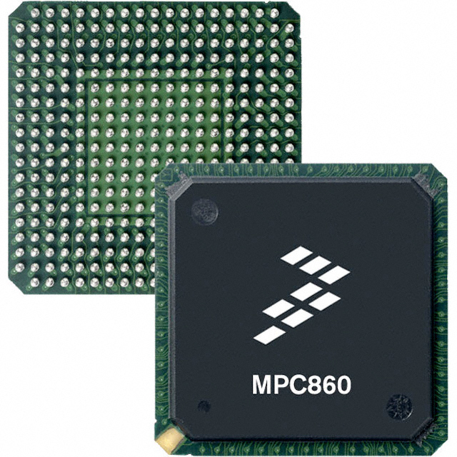
CPU32+ Microprocessor IC M683xx 1 Core, 32-Bit 33MHz 357-PBGA (25x25) |
|---|---|
| Quantity | 1,740 Available (as of October 8, 2026) |
| Product Category | Microprocessors |
|---|---|
| Part Series | MC68 |
| Manufacturer | NXP USA Inc. |
| Manufacturing Status | Obsolete |
| Manufacturer Standard Lead Time | Contact Us |
| Datasheet |
Specifications & Environmental
| Co-Processors/DSP | Communications; CPM | Core Processor | CPU32+ | Device Package | 357-PBGA (25x25) | ||
|---|---|---|---|---|---|---|---|
| ECCN | 3A991A2 | Ethernet | 10Mbps (1) | Graphics Acceleration | No | ||
| HTS Code | 8542.31.0001 | Moisture Sensitivity Level | 3 (168 Hours) | Mounting Method | Surface Mount | ||
| Mounting Type | Surface Mount | Number of Cores/Bus Width | 1 Core, 32-Bit | Operating Temperature | 0°C ~ 70°C (TA) | ||
| Package / Case | 357-BBGA | RAM Controllers | DRAM | REACH Compliance | REACH Unaffected | ||
| RoHS Compliance | ROHS3 Compliant | Speed | 33MHz | Supplier Device Package | 357-PBGA (25×25) | ||
| Voltage – I/O | 5.0V |
Overview of MC68EN360VR33L – IC MPU M683XX 33MHz 357BGA
The MC68EN360VR33L is a CPU32+ microprocessor delivering a single 32‑bit core operating at 33 MHz in a 357‑pin PBGA (25×25) surface‑mount package. Designed for embedded systems, this device integrates a communications‑oriented Communications Processor Module (CPM) and a suite of serial controllers to support complex protocol handling and network I/O.
With on‑chip DRAM controller support, integrated serial channels and DMA, and 5 V I/O, the MC68EN360VR33L targets embedded communications and control applications that require consolidated peripheral functionality and predictable operating characteristics across 0 °C to 70 °C.
Key Features
- Core and Performance — CPU32+ single 32‑bit core running at 33 MHz, providing a familiar CPU32 architecture for embedded software development.
- Voltage and Mounting — 5 V I/O logic levels with a surface‑mount 357‑pin PBGA (25×25) package for compact, board‑level integration.
- Communications Processor Module (CPM) — On‑chip CPM with a RISC controller and protocol support, designed to offload serial communications tasks and manage buffer descriptors for efficient data handling.
- Serial Interfaces — Multiple serial channels including four Serial Communications Controllers (SCCs), two Serial Management Controllers (SMCs) and one SPI, enabling versatile serial protocol connectivity and HDLC/SDLC support.
- Ethernet Support — Full 10 Mbps Ethernet/IEEE 802.3 support available on SCC1, providing an integrated network interface option for embedded networking designs.
- Memory and Bus — Support for dynamic bus sizing up to a 32‑bit data bus and DRAM controller options to interface with SRAM, EPROM, or Flash memory devices.
- Timers and DMA — Four general‑purpose timers (configurable as four 16‑bit or two 32‑bit timers) and two independent DMA controllers for high‑efficiency data transfers and precise timing control.
- System Integration and Diagnostics — System Integration Module features such as watchdog, bus monitoring, breakpoint logic and IEEE 1149.1 Test Access Port to aid system reliability and debug.
- Operating Range and Compliance — Commercial temperature operation from 0 °C to 70 °C and RoHS compliance for environmental conformance.
Typical Applications
- Embedded Communications Equipment — Ideal for modem controllers, protocol concentrators and communication gateways where on‑chip CPM and multiple serial channels accelerate packet handling and protocol offload.
- Network Interface Modules — Use SCC1 Ethernet capability and serial interfaces to implement 10 Mbps network endpoints and legacy serial‑to‑Ethernet bridges.
- Industrial Control and Automation — Integrate control, timing and serial I/O in compact embedded controllers that require deterministic timers and DMA for peripheral data movement.
- Protocol Conversion and Telecom — Support for HDLC/SDLC and multiple serial channels makes the device suited to protocol conversion, link termination and telecom interface modules.
Unique Advantages
- Highly integrated communications peripherals: On‑chip CPM plus SCC/SMC/SPI channels reduce external component count and simplify board design for serial and networked applications.
- Offloaded protocol processing: CPM with dedicated buffer descriptors enables efficient handling of serial protocols without continuous CPU intervention.
- Flexible memory interfacing: Dynamic bus sizing and DRAM controller support allow designers to match memory architectures (SRAM/EPROM/Flash) to application requirements.
- Deterministic I/O and timing: Multiple timers and independent DMA channels provide precise control and high‑throughput data movement for real‑time embedded tasks.
- Compact PBGA footprint: 357‑pin PBGA (25×25) package supports high pin density in space‑constrained embedded systems.
- Standards and environmental readiness: 10 Mbps Ethernet support on SCC1 and RoHS compliance align the device with common networking needs and regulatory expectations.
Why Choose MC68EN360VR33L?
The MC68EN360VR33L combines a CPU32+ 32‑bit core with a communications‑focused peripheral set—CPM, multiple serial controllers, DMA and DRAM interfacing—making it a practical choice for embedded designs that require integrated protocol handling and network connectivity. Its 33 MHz operation, surface‑mount PBGA package and commercial temperature range suit compact, production embedded systems.
This part is positioned for engineers seeking an integrated processor with on‑chip communications acceleration to reduce BOM and simplify system architecture, while retaining flexible memory and I/O options for a range of embedded networking and control applications.
Request a quote or submit an inquiry to receive pricing, availability and technical purchasing support for the MC68EN360VR33L.





















Date Founded: 2006
Headquarters: Eindhoven, North Brabant, Netherlands
Employees: 38,000+
Revenue: $10.53 Billion
Certifications and Memberships: ISO9001:2015, IATF16949:2016


