
MC68EN360VR25LR2
| Part Description |
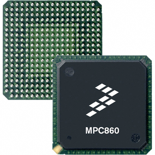
CPU32+ Microprocessor IC M683xx 1 Core, 32-Bit 25MHz 357-PBGA (25x25) |
|---|---|
| Quantity | 309 Available (as of October 8, 2026) |
| Product Category | Microprocessors |
|---|---|
| Part Series | MC68 |
| Manufacturer | NXP USA Inc. |
| Manufacturing Status | Obsolete |
| Manufacturer Standard Lead Time | Contact Us |
| Datasheet |
Specifications & Environmental
| Co-Processors/DSP | Communications; CPM | Core Processor | CPU32+ | Device Package | 357-PBGA (25x25) | ||
|---|---|---|---|---|---|---|---|
| ECCN | EAR99 | Ethernet | 10Mbps (1) | Graphics Acceleration | No | ||
| HTS Code | 8542.31.0001 | Moisture Sensitivity Level | 3 (168 Hours) | Mounting Method | Surface Mount | ||
| Mounting Type | Surface Mount | Number of Cores/Bus Width | 1 Core, 32-Bit | Operating Temperature | 0°C ~ 70°C (TA) | ||
| Package / Case | 357-BBGA | RAM Controllers | DRAM | REACH Compliance | REACH Unaffected | ||
| RoHS Compliance | ROHS3 Compliant | Speed | 25MHz | Supplier Device Package | 357-PBGA (25×25) | ||
| Voltage – I/O | 5.0V |
Overview of MC68EN360VR25LR2 – IC MPU M683XX 25 MHz 357‑PBGA (25×25)
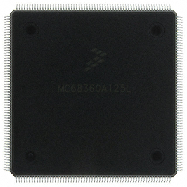
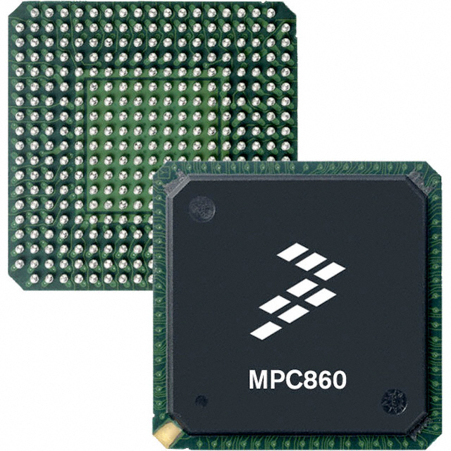
The MC68EN360VR25LR2 is a CPU32+ microprocessor IC featuring a single 32‑bit core running at 25 MHz, supplied in a 357‑pin PBGA (25×25) surface‑mount package. It integrates communications-focused elements and system integration functionality documented in the MC68360 QUICC user manual.
Designed for embedded applications that require integrated communications support, this device combines a CPU32+ core with a Communications Processor Module (CPM), DRAM controller support and a 10 Mbps Ethernet interface to simplify system design and accelerate time to market.
Key Features
- CPU Core & Performance — Single CPU32+ core, 32‑bit architecture operating at 25 MHz for deterministic embedded processing.
- Power & I/O — 5 V I/O voltage to match legacy and established embedded interfaces.
- Communications & Co‑Processing — Dedicated communications co‑processor (CPM) and DSP communications support for offloading serial and protocol tasks.
- Memory Interface — Integrated DRAM controller support to facilitate system memory interfacing.
- Networking — On‑chip 10 Mbps Ethernet interface (1) for basic network connectivity.
- Peripheral Interfaces — Additional serial interfaces including SCC for versatile serial connectivity.
- Package & Mounting — 357‑PBGA (25×25) supplier device package, surface mount for compact board designs.
- Operating Range — Rated for 0 °C to 70 °C operation and RoHS compliant for environmental compliance.
- Documentation — Supported by detailed MC68360 QUICC user manual content covering CPU32+, SIM60, CPM, memory maps, bus operation and programming.
Typical Applications
- Embedded Communications Controllers — Use the integrated CPM and serial interfaces to implement protocol offload and serial networking tasks.
- Network Edge and Access Devices — Leverage the on‑chip 10 Mbps Ethernet interface for basic network connectivity in edge or access equipment.
- Industrial Embedded Systems — Employ the 32‑bit CPU32+ core and DRAM controller support in compact, surface‑mount designs requiring reliable embedded processing.
- Serial Interface Gateways — Utilize SCC and CPM resources to bridge or aggregate serial communication links in embedded solutions.
Unique Advantages
- Integrated Communications Subsystem: The Communications Processor Module (CPM) provides dedicated offload for serial and protocol processing, reducing CPU overhead.
- Single 32‑Bit Core Architecture: CPU32+ 32‑bit processing delivers predictable performance for embedded control and protocol tasks.
- On‑board Memory Support: DRAM controller integration simplifies system memory design and reduces external component count.
- Compact Surface‑Mount PBGA Package: 357‑pin PBGA (25×25) packaging enables high‑density board layouts while supporting robust I/O connectivity.
- Documented Development Support: Comprehensive user manual material for CPU32+, SIM60 and CPM helps accelerate integration, programming and system validation.
- Regulatory and Environmental Compliance: RoHS compliance supports environmentally conscious product design and supply chain requirements.
Why Choose MC68EN360VR25LR2?
The MC68EN360VR25LR2 positions itself as an embedded microprocessor solution that balances a dedicated communications subsystem with a single CPU32+ core, offering a focused platform for designs requiring serial protocol handling, basic Ethernet connectivity and DRAM interfacing. Its 357‑pin PBGA package and surface‑mount mounting support compact board layouts common in embedded equipment.
This device is well suited to teams building embedded communications or control systems that benefit from documented MC68360 QUICC architecture material (CPU32+, SIM60, CPM) and require a RoHS‑compliant component rated for 0 °C to 70 °C operation. The integration of communications co‑processing, memory controller support and established I/O voltage simplifies BOM and system integration.
Request a quote or submit a purchase inquiry to obtain pricing, availability and lead‑time information for the MC68EN360VR25LR2.





















Date Founded: 2006
Headquarters: Eindhoven, North Brabant, Netherlands
Employees: 38,000+
Revenue: $10.53 Billion
Certifications and Memberships: ISO9001:2015, IATF16949:2016


