
MC68EN360ZQ25VL
| Part Description |
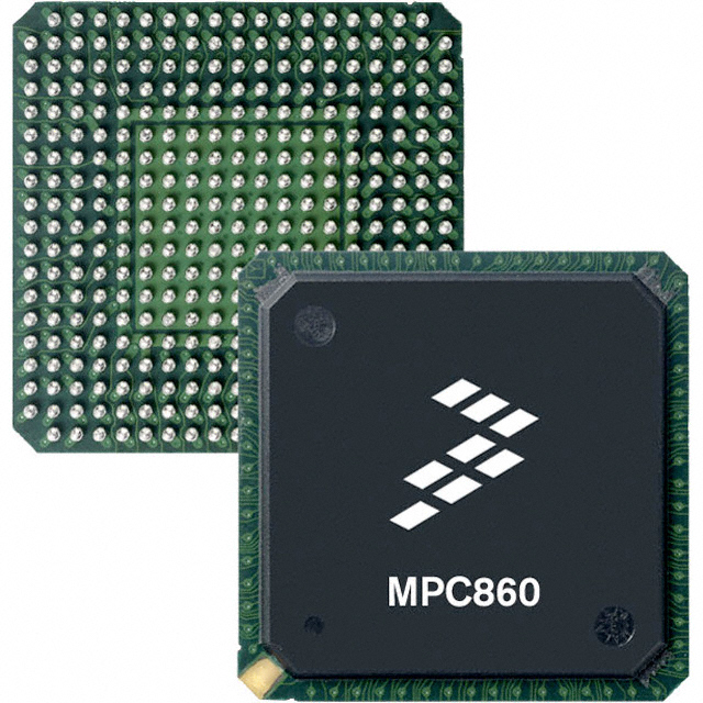
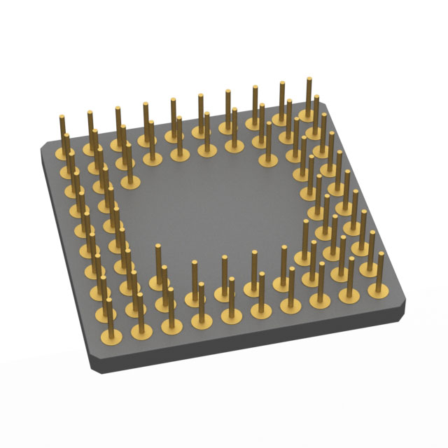
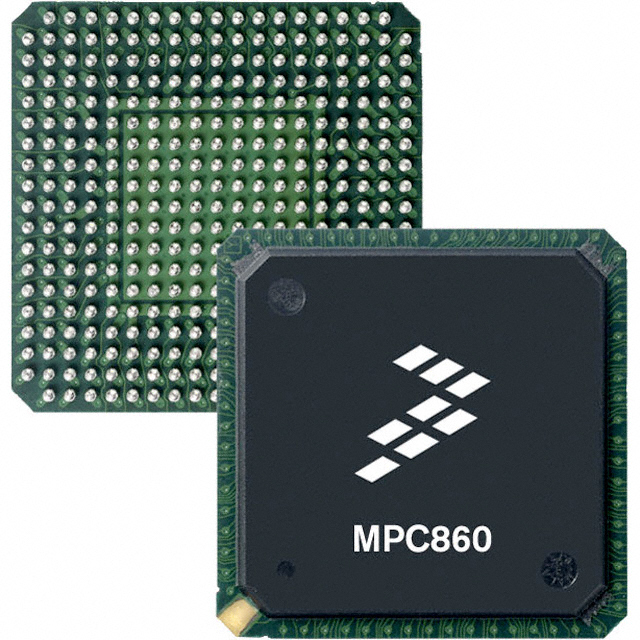
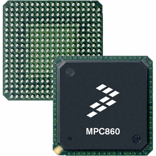
CPU32+ Microprocessor IC M683xx 1 Core, 32-Bit 25MHz 357-PBGA (25x25) |
|---|---|
| Quantity | 42 Available (as of October 8, 2026) |
| Product Category | Microprocessors |
|---|---|
| Part Series | MC68 |
| Manufacturer | NXP USA Inc. |
| Manufacturing Status | Obsolete |
| Manufacturer Standard Lead Time | Contact Us |
| Datasheet |
Specifications & Environmental
| Co-Processors/DSP | Communications; CPM | Core Processor | CPU32+ | Device Package | 357-PBGA (25x25) | ||
|---|---|---|---|---|---|---|---|
| ECCN | EAR99 | Ethernet | 10Mbps (1) | Graphics Acceleration | No | ||
| HTS Code | 8542.31.0001 | Moisture Sensitivity Level | 3 (168 Hours) | Mounting Method | Surface Mount | ||
| Mounting Type | Surface Mount | Number of Cores/Bus Width | 1 Core, 32-Bit | Operating Temperature | 0°C ~ 70°C (TA) | ||
| Package / Case | 357-BBGA | RAM Controllers | DRAM | REACH Compliance | REACH Unaffected | ||
| RoHS Compliance | RoHS non-compliant | Speed | 25MHz | Supplier Device Package | 357-PBGA (25×25) | ||
| Voltage – I/O | 3.3V |
Overview of MC68EN360ZQ25VL – IC MPU M683XX 25MHZ 357BGA
The MC68EN360ZQ25VL is a single-core CPU32+ microprocessor from NXP Semiconductors, operating at 25 MHz with a 32-bit core architecture. Designed for embedded controller and communications-focused applications, it integrates a Communications Processor Module (CPM) and multiple serial controllers to simplify protocol handling and system integration.
This device targets embedded and communications markets where integrated serial interfaces, on-chip system management, and a compact 357-PBGA (25×25) surface-mount package are valued. Key value comes from its integrated communications peripherals, flexible memory/bus support and on-chip system reliability features.
Key Features
- CPU Core: CPU32+ single 32-bit core running at 25 MHz delivering approximately 4.5 MIPS at 25 MHz as specified for the CPU32+ implementation.
- Bus and Memory Support: Up to 32-bit data bus with dynamic bus sizing for 8- and 16-bit operation and up to 32 address lines; supports external memory types including SRAM, EPROM, Flash and DRAM with multiple CAS/WE/OE signals and boot chip select options.
- Communications Processor Module (CPM): Integrated RISC-based CPM with 224 buffer descriptors and support for continuous transmit/receive modes to offload serial protocol processing.
- Serial Interfaces: Four Serial Communications Controllers (SCCs), two Serial Management Controllers (SMCs) and one SPI; SCC1 offers optional Ethernet (IEEE 802.3) support at full 10 Mbps on the MC68EN360 variant.
- DMA and Timers: Two independent DMAs with buffer chaining, auto buffer modes and efficient packing; four general-purpose timers configurable as four 16-bit or two 32-bit timers with gate mode.
- System Integration Module (SIM60): On-chip features including bus monitor, double bus fault monitor, spurious interrupt monitor, software watchdog, periodic interrupt timer, clock synthesizer and breakpoint logic.
- Debug and Test: Background Debug Mode and IEEE 1149.1 Test Access Port for on-chip debug and boundary-scan testing.
- Power and Packaging: 3.3 V IO supply, surface-mount 357-PBGA (25×25) package, and a Low Power Stop Mode for reduced power operation.
- Operating Range and Compliance: Rated for 0 °C to 70 °C operation and RoHS compliant.
Typical Applications
- Embedded Communications Controllers: Offload protocol handling and serial channel management using the integrated CPM and multiple SCC/SMC channels.
- Network Interface Modules: Implement 10 Mbps Ethernet on SCC1 and manage HDLC/SDLC channels for networked embedded systems.
- Industrial and Control Systems: Use on-chip timers, DMA and robust bus monitoring features for deterministic control and data movement.
Unique Advantages
- Highly integrated communications capability: Multiple SCCs, SMCs, SPI and a CPM reduce external component count and simplify protocol implementations.
- Flexible memory and bus options: Dynamic bus sizing and support for various external memory types enable straightforward interface to existing memory designs.
- On-chip system reliability features: Built-in watchdog, bus fault monitors and spurious interrupt monitoring help detect and recover from system faults.
- Compact surface-mount package: 357-PBGA (25×25) package provides a compact footprint for space-constrained board designs.
- Standard voltage and industry compliance: 3.3 V IO and RoHS compliance simplify integration into modern embedded systems.
Why Choose MC68EN360ZQ25VL?
The MC68EN360ZQ25VL delivers a balanced combination of a CPU32+ 32-bit core, comprehensive communications peripherals and system integration features suitable for embedded controllers focused on serial communications and network interfacing. Its integrated CPM, multiple serial channels and DMA support reduce external logic and simplify firmware implementation for protocol-heavy applications.
Engineers designing communications modules, network interfaces or industrial controllers will find the device’s on-chip reliability features, flexible memory interface and compact 357-PBGA package advantageous for building robust, space-efficient systems operating across a 0 °C to 70 °C range.
Request a quote or submit a purchasing inquiry to receive pricing and availability information for the MC68EN360ZQ25VL.





















Date Founded: 2006
Headquarters: Eindhoven, North Brabant, Netherlands
Employees: 38,000+
Revenue: $10.53 Billion
Certifications and Memberships: ISO9001:2015, IATF16949:2016


