
MC68EN360ZP25VL
| Part Description |
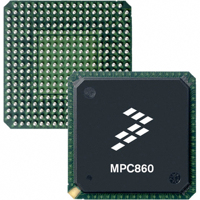
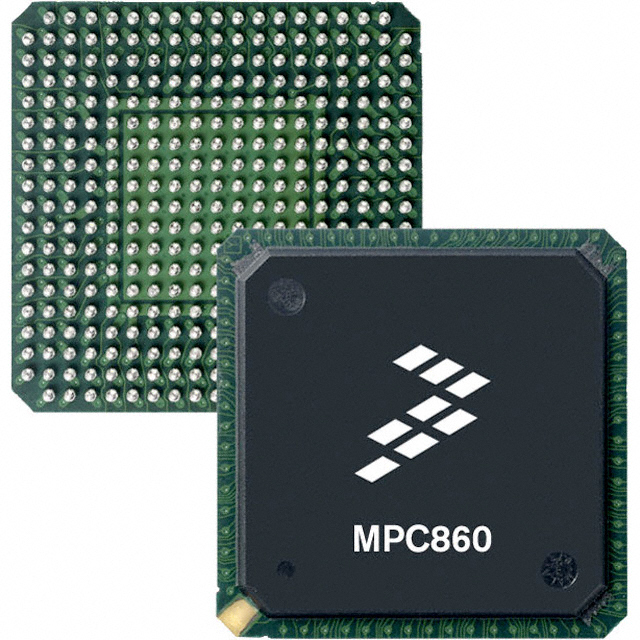
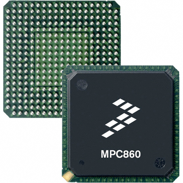
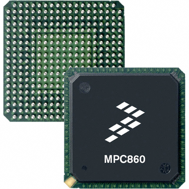
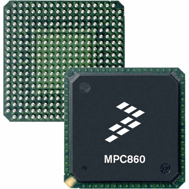
CPU32+ Microprocessor IC M683xx 1 Core, 32-Bit 25MHz 357-PBGA (25x25) |
|---|---|
| Quantity | 108 Available (as of October 8, 2026) |
| Product Category | Microprocessors |
|---|---|
| Part Series | MC68 |
| Manufacturer | NXP USA Inc. |
| Manufacturing Status | Obsolete |
| Manufacturer Standard Lead Time | Contact Us |
| Datasheet |
Specifications & Environmental
| Co-Processors/DSP | Communications; CPM | Core Processor | CPU32+ | Device Package | 357-PBGA (25x25) | ||
|---|---|---|---|---|---|---|---|
| ECCN | EAR99 | Ethernet | 10Mbps (1) | Graphics Acceleration | No | ||
| HTS Code | 8542.31.0001 | Moisture Sensitivity Level | 3 (168 Hours) | Mounting Method | Surface Mount | ||
| Mounting Type | Surface Mount | Number of Cores/Bus Width | 1 Core, 32-Bit | Operating Temperature | 0°C ~ 70°C (TA) | ||
| Package / Case | 357-BGA | RAM Controllers | DRAM | REACH Compliance | REACH Unaffected | ||
| RoHS Compliance | RoHS non-compliant | Speed | 25MHz | Supplier Device Package | 357-PBGA (25×25) | ||
| Voltage – I/O | 3.3V |
Overview of MC68EN360ZP25VL – CPU32+ 25 MHz 357-PBGA Microprocessor
The MC68EN360ZP25VL is a CPU32+ microprocessor in the MC68 series, featuring a single 32‑bit core running at 25 MHz and designed for embedded communications-centric applications. It integrates system and communications functionality drawn from the MC68360 QUICC family, with on-chip communications processing and system integration modules that simplify embedded networking and control designs.
Key value comes from its integrated communications coprocessor (CPM), DRAM controller, and on-chip 10 Mbps Ethernet interface, combined with industry-standard 357‑PBGA (25 × 25) surface‑mount packaging and 3.3 V I/O compatibility for straightforward system integration.
Key Features
- CPU Core CPU32+ single 32‑bit core running at 25 MHz, providing deterministic embedded processing for control and communications tasks.
- Communications Processor Module (CPM) On‑chip communications coprocessor functionality to offload serial and protocol handling from the main CPU, enabling efficient data handling.
- Memory Support Includes DRAM controller support to interface with external system memory for application and data storage.
- Ethernet Integrated 10 Mbps Ethernet interface (1 port) for basic network connectivity in embedded systems.
- Serial and Peripheral Interfaces Additional serial controller interfaces such as SCC and other QUICC serial configurations referenced in the product documentation for flexible I/O options.
- System Integration On‑chip System Integration Module (SIM60) and support infrastructure described in the MC68360 family documentation, aiding board‑level integration and system design.
- Package and Mounting 357‑PBGA package (25 × 25) in a surface‑mount format for compact board layouts and reliable soldered assembly.
- Electrical 3.3 V I/O voltage for compatibility with standard embedded logic levels.
- Operating Conditions Commercial temperature range 0 °C to 70 °C suitable for standard industrial and commercial applications.
- Standards and Testability Documentation for IEEE 1149.1 Test Access Port is included in the MC68360 family user manual, supporting boundary‑scan test strategies.
- Environmental Compliance RoHS compliant for reduced environmental impact in manufacturing and assembly.
Typical Applications
- Networking and Communications Equipment Use the built‑in CPM and 10 Mbps Ethernet interface for embedded network controllers and protocol handling.
- Industrial Control CPU32+ performance with DRAM support and robust serial interfaces for machine control, supervisory systems, and field controllers.
- Embedded Systems Compact PBGA packaging and 3.3 V I/O make the device suitable for space‑constrained embedded products requiring integrated communications.
- Telecommunications Modules Integrated communications processing and serial configurations address tasks such as link management and peripheral interfacing in telecom modules.
Unique Advantages
- Integrated Communications Processing: CPM and QUICC‑family architecture reduce host CPU load by handling serial and protocol tasks on‑chip.
- Simplified Memory Interface: Built‑in DRAM controller streamlines system memory integration and reduces external glue logic.
- Compact, Industry‑Ready Packaging: 357‑PBGA (25 × 25) surface‑mount package enables dense board layouts while maintaining solderability for production volumes.
- Standard Logic Levels: 3.3 V I/O ensures direct compatibility with common embedded peripherals and interfaces.
- Documented Architecture: The MC68360 family documentation (user manual and programmer’s reference) provides architectural and programming detail to accelerate development.
- RoHS Compliant: Helps meet environmental regulations and corporate supply‑chain requirements.
Why Choose MC68EN360ZP25VL?
The MC68EN360ZP25VL positions itself as an integrated communications‑centric microprocessor for embedded designs that need a CPU32+ core with on‑chip communications processing, memory controller support, and basic Ethernet connectivity. Its combination of CPM functionality, DRAM interfacing, and documented QUICC architecture supports designs where embedded networking and serial protocol handling are central requirements.
This device is well suited for teams seeking a documented, RoHS‑compliant processor in a compact 357‑PBGA package with 3.3 V I/O and a commercial operating range. The available family user manual and programmer’s reference materials help accelerate integration and software development for targeted communications and embedded control applications.
Request a quote or submit a purchasing inquiry to receive pricing and availability for the MC68EN360ZP25VL. Provide your volume and delivery requirements to get a tailored response.





















Date Founded: 2006
Headquarters: Eindhoven, North Brabant, Netherlands
Employees: 38,000+
Revenue: $10.53 Billion
Certifications and Memberships: ISO9001:2015, IATF16949:2016


