
MCIMX6X2EVN10ABR
| Part Description |
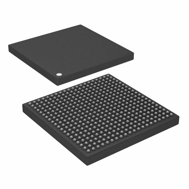
ARM® Cortex®-A9, ARM® Cortex®-M4 Microprocessor IC i.MX6SX 2 Core, 32-Bit 227MHz, 1GHz 400-MAPBGA (17x17) |
|---|---|
| Quantity | 571 Available (as of October 9, 2026) |
| Product Category | Microprocessors |
|---|---|
| Part Series | i.MX 6X |
| Manufacturer | NXP USA Inc. |
| Manufacturing Status | Not For New Designs |
| Manufacturer Standard Lead Time | 15 Weeks |
| Datasheet |
Specifications & Environmental
| Co-Processors/DSP | Multimedia; NEON™ MPE | Core Processor | ARM® Cortex®-A9, ARM® Cortex®-M4 | Device Package | 400-MAPBGA (17x17) | ||
|---|---|---|---|---|---|---|---|
| Display & Interface Controllers | Keypad, LCD | ECCN | 5A992C | Ethernet | 10/100/1000Mbps (2) | ||
| Graphics Acceleration | Yes | HTS Code | 8542.31.0001 | Moisture Sensitivity Level | 3 (168 Hours) | ||
| Mounting Method | Surface Mount | Mounting Type | Surface Mount | Number of Cores/Bus Width | 2 Core, 32-Bit | ||
| Operating Temperature | -20°C ~ 105°C (TJ) | Package / Case | 400-LFBGA | RAM Controllers | LPDDR2, LVDDR3, DDR3 | ||
| REACH Compliance | REACH Unaffected | RoHS Compliance | ROHS3 Compliant | Security Features | A-HAB, ARM TZ, CAAM, CSU, SNVS, System JTAG, TVDECODE | ||
| Speed | 227MHz, 1GHz | Supplier Device Package | 400-MAPBGA (17×17) | USB | USB 2.0 + PHY (1), USB 2.0 OTG + PHY (2) | ||
| Voltage – I/O | 1.8V, 2.5V, 2.8V, 3.15V |
Overview of MCIMX6X2EVN10ABR – IC MPU I.MX6SX 1GHZ 400-MAPBGA
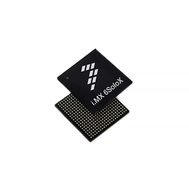
The MCIMX6X2EVN10ABR is an NXP i.MX 6X series microprocessor IC that combines an ARM® Cortex®-A9 application core with an ARM® Cortex®-M4 real-time core in a heterogeneous multicore architecture. The device targets multimedia-focused and connected products that require integrated processing, graphics acceleration, and a broad set of peripheral interfaces.
With a Cortex‑A9 core operating up to 1 GHz and a Cortex‑M4 core operating up to 227 MHz, the part delivers a balance of high‑performance application processing and fast real‑time responsiveness, along with integrated power management and security features for system-level integration.
Key Features
- Core Architecture Heterogeneous dual‑core design: ARM Cortex‑A9 (up to 1 GHz) paired with ARM Cortex‑M4 (227 MHz) for combined application and real‑time processing.
- Memory Interfaces Supports LPDDR2, LVDDR3 and DDR3 memory controllers for flexible system memory choices.
- Multimedia & Graphics Includes graphics acceleration and an integrated GPU capable of supporting 2D and 3D operations for display and HMI applications.
- Connectivity Dual Gigabit Ethernet controllers (10/100/1000 Mbps x2) and multiple USB controllers (USB 2.0 + PHY x1, USB 2.0 OTG + PHY x2) to support high‑bandwidth wired interfaces.
- Display & Audio Display interface controllers include LCD and keypad support; additional audio interface AC'97 is available for legacy audio connectivity.
- Security & Debug Hardware security features: A‑HAB, ARM TrustZone (ARM TZ), CAAM, CSU, SNVS, System JTAG, and TVDECODE for secure boot and system integrity functions.
- Power & Low‑Power Operation Integrated power management and “smart low‑power system awareness” to support power‑sensitive designs.
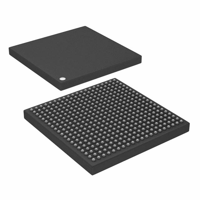
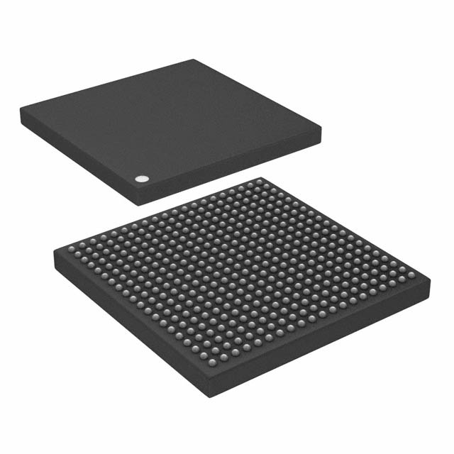
- Package & Temperature Supplied in a 400‑MAPBGA (17 × 17 mm) surface‑mount package; operating temperature range −20 °C to 105 °C.
- Compliance RoHS compliant.
Typical Applications
- Consumer Multimedia Devices Application and graphics processing for multimedia‑focused consumer products with integrated display and audio support.
- Connected Devices Gateway and connected device designs that require application processing alongside real‑time control and secure connectivity.
- Human‑Machine Interfaces HMI platforms leveraging LCD and keypad interfaces plus GPU acceleration for smooth 2D/3D graphics.
- Imaging and Sensor Systems Systems integrating displays and camera sensors where combined application and real‑time processing benefits image handling and control.
Unique Advantages
- Heterogeneous Processing: Combines a high‑speed Cortex‑A9 core (up to 1 GHz) with a Cortex‑M4 real‑time core (227 MHz) to separate application workloads from deterministic control tasks.
- Integrated Multimedia Subsystem: GPU and graphics acceleration plus display and audio interfaces reduce the need for external video processing components.
- Flexible Memory Support: Native support for LPDDR2, LVDDR3 and DDR3 memory types enables designers to select memory optimized for performance, cost, or power.
- Comprehensive Connectivity: Dual Gigabit Ethernet and multiple USB PHYs provide robust wired connectivity options for high‑throughput applications.
- Hardware Security Suite: On‑chip security features (A‑HAB, ARM TZ, CAAM, CSU, SNVS) support secure boot and system integrity for connected and embedded applications.
- Production‑Ready Packaging and Range: 400‑MAPBGA package with an industrial operating range (−20 °C to 105 °C) suitable for a wide range of embedded environments.
Why Choose MCIMX6X2EVN10ABR?
The MCIMX6X2EVN10ABR positions itself as a highly integrated solution for designs that require both application‑level performance and real‑time responsiveness. Its combination of a 1 GHz Cortex‑A9 core and a 227 MHz Cortex‑M4 core, together with on‑chip graphics acceleration, flexible memory interfaces, rich connectivity and hardware security, supports multimedia‑focused, connected applications with reduced external BOM.
This device is suited to developers building consumer multimedia products, connected devices, HMIs and imaging systems that benefit from integrated power management, secure boot capabilities and a broad peripheral set provided in a 400‑MAPBGA package.
Request a quote or submit a purchase inquiry to receive pricing and availability information for the MCIMX6X2EVN10ABR.



















Date Founded: 2006
Headquarters: Eindhoven, North Brabant, Netherlands
Employees: 38,000+
Revenue: $10.53 Billion
Certifications and Memberships: ISO9001:2015, IATF16949:2016


