
MCIMX6Y0DVM05AA
| Part Description |
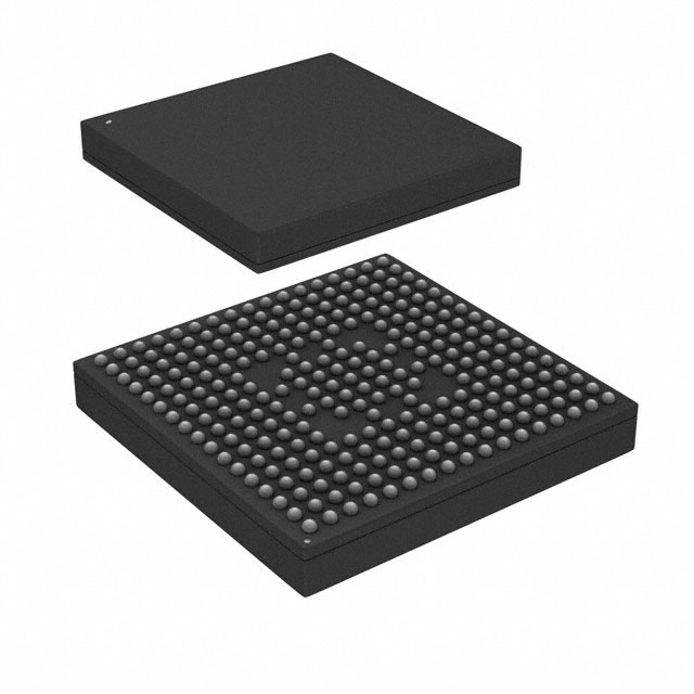
ARM® Cortex®-A7 Microprocessor IC i.MX6 1 Core, 32-Bit 528MHz 289-MAPBGA (14x14) |
|---|---|
| Quantity | 199 Available (as of October 9, 2026) |

| Product Category | Microprocessors |
|---|---|
| Part Series | i.MX 6Y |
| Manufacturer | NXP USA Inc. |
| Manufacturing Status | Active |
| Manufacturer Standard Lead Time | 16 Weeks |
| Datasheet |
Specifications & Environmental
| Co-Processors/DSP | Multimedia; NEON™ MPE | Core Processor | ARM® Cortex®-A7 | Device Package | 289-MAPBGA (14x14) | ||
|---|---|---|---|---|---|---|---|
| Display & Interface Controllers | Electrophoretic, LCD | ECCN | 5A992C | Ethernet | 10/100Mbps (1) | ||
| Graphics Acceleration | No | HTS Code | 8542.31.0001 | Moisture Sensitivity Level | 3 (168 Hours) | ||
| Mounting Method | Surface Mount | Mounting Type | Surface Mount | Number of Cores/Bus Width | 1 Core, 32-Bit | ||
| Operating Temperature | 0°C ~ 95°C (TJ) | Package / Case | 289-LFBGA | RAM Controllers | LPDDR2, DDR3, DDR3L | ||
| REACH Compliance | REACH Unaffected | RoHS Compliance | ROHS3 Compliant | Security Features | A-HAB, ARM TZ, CSU, SJC, SNVS | ||
| Speed | 528MHz | Supplier Device Package | 289-MAPBGA (14×14) | USB | USB 2.0 OTG + PHY (1) | ||
| Voltage – I/O | 1.8V, 2.8V, 3.3V |
Overview of MCIMX6Y0DVM05AA – ARM Cortex‑A7 528 MHz MPU, 289‑MAPBGA
The MCIMX6Y0DVM05AA is a single‑core ARM® Cortex®‑A7 microprocessor IC operating at 528 MHz, designed for embedded and consumer‑oriented connected devices. It combines a 32‑bit Cortex‑A7 core with multimedia co‑processor support and integrated system features to simplify designs that require efficient application processing and peripheral connectivity.
As part of the i.MX 6Y series and i.MX 6ULL family, this device targets consumer and connected device applications where integration, security, and flexible memory and interface options are important design considerations.
Key Features
- Core Single ARM® Cortex®‑A7 32‑bit core running at 528 MHz for general purpose embedded application processing.
- Multimedia Accelerators Includes multimedia co‑processors with NEON™ MPE support for accelerated media and signal processing tasks.
- Memory Interfaces Supports LPDDR2, DDR3 and DDR3L memory controllers to accommodate a range of system memory choices.
- Display Support Display interface controllers for electrophoretic and LCD panels suitable for user interface and low‑power display applications.
- Connectivity Integrated 10/100 Mbps Ethernet (1) and USB 2.0 OTG with PHY (1) plus I²C for common peripheral and network connectivity.
- Security Features Hardware security elements including A‑HAB, ARM TrustZone (ARM TZ), CSU, SJC, and SNVS for secure boot and trusted execution.
- Power and Integration Part of a family that includes an integrated power management module to reduce external power supply complexity.
- Package and Mounting Available in a 289‑MAPBGA supplier package (14 × 14 mm) and listed package case 289‑LFBGA; surface mount device for compact board designs.
- Operating Range & Compliance Rated for operation from 0 °C to 95 °C and RoHS compliant for consumer and embedded applications.
Typical Applications
- Consumer Devices Application processing and peripheral control in consumer electronics that require a compact, single‑core embedded MPU.
- Connected Devices Edge devices and IoT‑class products leveraging Ethernet, USB OTG and I²C connectivity for networked sensor and gateway functions.
- Human‑Machine Interfaces (HMI) Driving electrophoretic or LCD displays for user interfaces where efficient display control and multimedia support are needed.
- Multimedia‑Enabled Embedded Systems Systems using NEON™ MPE and multimedia co‑processors for lightweight media processing tasks within consumer and connected applications.
Unique Advantages
- Integrated Security Suite: On‑chip A‑HAB, ARM TrustZone, CSU, SJC and SNVS provide a comprehensive hardware security foundation for secure boot and trusted applications.
- Flexible Memory Support: Native controllers for LPDDR2, DDR3 and DDR3L enable designers to choose memory technologies that match performance and power targets.
- Compact, Surface‑Mount Package: 289‑MAPBGA (14 × 14 mm) packaging supports high‑density board layouts for space‑constrained designs.
- Integrated Power Management (family feature): Built‑in power management capabilities in the i.MX 6ULL family simplify external power design and sequencing.
- Broad Peripheral Connectivity: Onboard Ethernet, USB OTG with PHY and I²C support common networking and peripheral interfacing needs without extensive external components.
- Consumer‑Focused Qualification: Qualification for consumer applications aligns the device with typical consumer product lifecycles and design requirements.
Why Choose MCIMX6Y0DVM05AA?
The MCIMX6Y0DVM05AA delivers a balanced combination of single‑core Cortex‑A7 processing, multimedia co‑processor support, and integrated system features tailored for embedded and consumer connected devices. Its flexible memory interfaces, built‑in security elements, and compact MAPBGA packaging make it suitable for designs that require efficient application processing and reliable peripheral integration.
As part of the NXP i.MX 6ULL family, the device offers integration and scalability for developers building consumer and connected products, helping to streamline BOM and board‑level complexity while providing hardware security and connectivity options for production designs.
Request a quote or submit a purchasing inquiry to evaluate MCIMX6Y0DVM05AA for your next embedded or consumer connected application.






















Date Founded: 2006
Headquarters: Eindhoven, North Brabant, Netherlands
Employees: 38,000+
Revenue: $10.53 Billion
Certifications and Memberships: ISO9001:2015, IATF16949:2016


